
Datasheet


DS28E04-100: 4096-Bit 1-Wire Addressable EEPROM with PIO
15 of 37
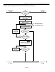
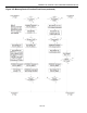
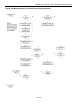
Figure 9-2. Memory/Control Function Flow Chart (continued)
AAh
Read Scratch-
Pad ?
DS28E04 sets Scratchpad
Offset = (T4:T0)
Bus Master RX
TA1 (T7:T0), TA2 (T15:T8)
and E/S Byte
Bus Master RX Data Byte
from Scratchpad Offset
Bus Master RX CRC16
of Command, Address,
E/S Byte, Data Bytes as
sent by the DS28E04
Y
Bus Master
RX “1”s
Master
TX Reset ?
Y
N
Master
TX Reset ?
DS28E04
Increments
Scratchpad
Offset
Scrpad. Offset
= E4:E0 ?
Y
Y
N
N
N
From Figure 9
1
st
Part
To Figure 9
1
st
Part
To Figure 9
3
rd
Part
From Figure 9
3
rd
Part
See note in Write
Scratchpad flow chart
for additional details.