
Datasheet


DS28E04-100: 4096-Bit 1-Wire Addressable EEPROM with PIO
14 of 37
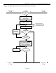
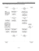
Figure 9-1. Memory/Control Function Flow Chart
0Fh
Write Scratch-
pad ?
Bus Master TX EEPROM
Array Target Address
TA1 (T7:T0), TA2 (T15:T8)
Y
N
To Figure 9
2
nd
Part
From Figure 9
2
nd
Part
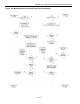
Bus Master TX Memory
Function Command
To ROM Functions
Flow Chart (Figure 14)
From ROM Functions
Flow Chart (Figure 14)
Master
TX Reset ?
Master TX Data Byte
To Scratchpad Offset
N
Y
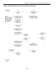
DS28E04 sets Scratchpad
Offset = (T4:T0),
Clears PF, AA
Scrpad. Offset
= 11111b?
DS28E04 TX CRC16
of Command, Address,
Data Bytes as they were
sent by the bus master
DS28E04
Increments
Scratchpad
Offset
Master
TX Reset ?
Y
N
Bus Master
RX “1”s
N
Partial
Byte ?
PF = 1
Y
N
Y
Applies only if the page is not write
protected or in EPROM mode. If write-
protected, then the DS28E04 copies the
data byte from the target address into
the scratchpad. If in EPROM mode,
then the DS28E04 stores the bitwise
logical AND of the transmitted byte and
the data byte from the targeted address
into the scratchpad.