
Datasheet


DS2780 Standalone Fuel Gauge IC
2 of 31
ABSOLUTE MAXIMUM RATINGS
Voltage Range on Any Pin Relative to VSS -0.3V to +6.0V
Voltage on VIN Relative to VSS -0.3V to (V
DD
+ 0.3V)
Operating Temperature Range
-40°C to +85°C
Storage Temperature Range
-55°C to +125°C
Soldering Temperature (10s)
See JEDEC J-STD-020
Stresses beyond those listed under “Absolute Maximum Ratings” may cause permanent damage to the device. These are stress ratings only,
and functional operation of the device at these or any other conditions beyond those indicated in the operational sections of the specifications is
not implied. Exposure to the absolute maximum rating conditions for extended periods may affect device reliability.
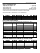
RECOMMENDED DC OPERATING CHARACTERISTICS
(VDD = 2.5V to 4.5V, T
A
= -20°C to +70°C, unless otherwise noted. Typical values are at T
A
= +25°C.)
PARAMETER SYMBOL CONDITIONS MIN TYP MAX UNITS
Supply Voltage VDD (Note 1) +2.5 +4.5 V
OVD Voltage (Note 1) -0.3 +4.5 V
DQ, PIO Voltage Range (Note 1) -0.3 +5.5 V
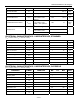
DC ELECTRICAL CHARACTERISTICS
(VDD = 2.5V to 4.5V, T
A
= -20°C to +70°C, unless otherwise noted. Typical values are at T
A
= +25°C.)
PARAMETER SYMBOL CONDITIONS MIN TYP MAX UNITS
2.5V ≤ VDD ≤ 4.2V 65 95
ACTIVE Current I
ACTIVE
105
µA
SLEEP Mode Current I
SLEEP
2.5V ≤ VDD ≤ 4.2V 1 3 µA
Input Logic High: DQ, PIO V
IH
(Note 1) 1.5 V
Input Logic Low: DQ, PIO V
IL
(Note 1) 0.6 V
Output Logic Low: DQ, PIO V
OL
I
OL
= 4mA (Note 1) 0.4 V
Pulldown Current: DQ, PIO I
PD
V
DQ
, V
PIO
= 0.4V 0.2 µA
Input Logic High: OVD V
IH
(Note 1)
VDD –
0.2
V
Input Logic Low: OVD V
IL
(Note 1) VSS + 0.2 V
VIN Input Resistance R
IN
15
M
DQ Capacitance C
DQ
50 pF
DQ SLEEP Timeout t
SLEEP
DQ < V
IL
(Note 5) 1.5 2.0 2.5 s
Undervoltage SLEEP
Threshold
V
SLEEP
(Note 1) 2.40 2.45 2.50 V
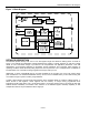
ELECTRICAL CHARACTERISTICS: TEMPERATURE, VOLTAGE, CURRENT
(V
CC
= 2.5V to 4.5V, T
A
= -20°C to +70°C, unless otherwise noted. Typical values are at T
A
= +25°C.)
PARAMETER SYMBOL CONDITIONS MIN TYP MAX UNITS
Temperature Resolution T
LSB
0.125 °C
Temperature Error T
ERR
±3 °C
Voltage Resolution V
LSB
4.88 mV
Voltage Full-Scale V
FS
0 4.992 V
Voltage Error V
ERR
±50 mV
Current Resolution I
LSB
1.56 µV