
Datasheet


Maxim Integrated | 4www.maximintegrated.com
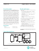
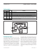
DS2482-100
Single-Channel 1-Wire Master
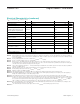
Note 1: Operating current with 1-Wire write-byte sequence followed by continuously reading the Status Register at 400kHz in overdrive.
Note 2: With standard speed, the total capacitive load of the 1-Wire bus should not exceed 1nF. Otherwise, the passive pullup on
threshold V
IL1
may not be reached in the available time. With overdrive speed, the capacitive load on the 1-Wire bus must
not exceed 300pF.
Note 3: Active pullup guaranteed to turn on between V
IL1(MAX)
and V
IH1(MIN)
.
Note 4: Active or resistive pullup choice is configurable.
Note 5: Except for t
F1
, all 1-Wire timing specifications and t
APUOT
are derived from the same timing circuit. Therefore, if one of
these parameters is found to be off the typical value, it is safe to assume that all these parameters deviate from their typi-
cal value in the same direction and by the same degree.
Note 6: These values apply at full load, i.e., 1nF at standard speed and 0.3nF at overdrive speed. For reduced load, the pulldown
slew rate is slightly faster.
Note 7: Fall time high-to-low (t
F1
) is derived from PD
SRC
, referenced from 0.9 x V
CC
to 0.1 x V
CC
.
Note 8: All I
2
C timing values are referred to V
IH(MIN)
and V
IL(MAX)
levels.
Note 9: Applies to SDA, SCL, AD0 and AD1.
Note 10: The input/output pins of the DS2482-100 do not obstruct the SDA and SCL lines if V
CC
is switched off.
Note 11: The DS2482-100 provides a hold time of at least 300ns for the SDA signal (referred to the V
IH(MIN)
of the SCL signal) to
bridge the undefined region of the falling edge of SCL.
Note 12: The maximum t
HD:DAT
need only be met if the device does not stretch the low period (t
LOW
) of the SCL signal.
Note 13: A fast-mode I
2
C bus device can be used in a standard-mode I
2
C bus system, but the requirement t
SU:DAT
≥ 250ns must
then be met. This is automatically the case if the device does not stretch the low period of the SCL signal. If such a device
does stretch the low period of the SCL signal, it must output the next data bit to the SDA line t
R(MAX)
+ t
SU:DAT
= 1000 +
250 = 1250ns (according to the standard-mode I
2
C bus specification) before the SCL line is released.
Note 14: C
B
—Total capacitance of one bus line in pF. If mixed with high-speed-mode devices, faster fall times according to
I
2
C-
Bus Specification Version 2.1
are allowed.
Note 15: I
2
C communication should not take place for the max t
OSCWUP
time following a power-on reset.
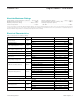
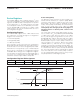
Electrical Characteristics (continued)
(V
CC
= 2.9V to 5.5V, T
A
= -40°C to +85°C.
)
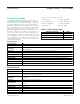
PARAMETER SYMBOL CONDITIONS MIN TYP MAX UNITS
Input Capacitance C
I
(Note 9) 10 pF
SCL Clock Frequency f
SCL
0 400 kHz
Hold Time (Repeated) START
Condition (After this period, the
first clock pulse is generated.)
t
HD:STA
0.6 μs
Low Period of the SCL Clock t
LOW
1.3 μs
High Period of the SCL Clock t
HIGH
0.6 μs
Setup Time for a Repeated
START Condition
t
SU:STA
0.6 μs
Data Hold Time t
HD:DAT
(Notes 11, 12) 0.9 μs
Data Setup Time t
SU:DAT
(Note 13) 250 ns
Setup Time for STOP Condition t
SU:STO
0.6 μs
Bus Free Time Between a STOP
and START Condition
t
BUF
1.3 μs
Capacitive Load for Each Bus
Line
C
B
(Note 14) 400 pF
Oscillator Warmup Time t
OSCWUP
(Note 15) 100 μs