
Datasheet


Read Scratchpad [AAh]
The Read Scratchpad command allows verifying the tar-
get address and the integrity of the scratchpad data. After
issuing the command code, the master begins reading.
The first two bytes are the target address. The next byte
is the ending offset/data status byte (E/S) followed by the
scratchpad data, which may be different from what the
master originally sent. This is of particular importance if
the target address is within the register page or a page
in either write-protection mode or EPROM mode. See the
Write Scratchpad [0Fh] section for details. The master
should read through the scratchpad (E[2:0] - T[2:0] + 1
bytes), after which it receives the inverted CRC based on
data as it was sent by the DS2431. If the master continues
reading after the CRC, all data is logic 1.
Copy Scratchpad [55h]
The Copy Scratchpad command is used to copy data
from the scratchpad to writable memory sections. After
issuing the Copy Scratchpad command, the master must
provide a 3-byte authorization pattern, which should
have been obtained by an immediately preceding Read
Scratchpad command. This 3-byte pattern must exactly
match the data contained in the three address registers
(TA1, TA2, E/S, in that order). If the pattern matches, the
target address is valid, the PF flag is not set, and the tar-
get memory is not copy protected, then the AA flag is set
and the copy begins. All 8 bytes of scratchpad contents
are copied to the target memory location. The duration
of the device’s internal data transfer is t
PROG
during
which the voltage on the 1-Wire bus must not fall below
2.8V. A pattern of alternating 0s and 1s are transmitted
after the data has been copied until the master issues a
reset pulse. If the PF flag is set or the target memory is
copy protected, the copy does not begin and the AA flag
is not set.
Read Memory [F0h]
The Read Memory command is the general function to
read data from the DS2431. After issuing the command,
the master must provide the 2-byte target address. After
these 2 bytes, the master reads data beginning from the
target address and can continue until address 008Fh. If
the master continues reading, the result is logic 1s. The
device’s internal TA1, TA2, E/S, and scratchpad contents
are not affected by a Read Memory command.
1-Wire Bus System
The 1-Wire bus is a system that has a single bus master
and one or more slaves. In all instances the DS2431 is
a slave device. The bus master is typically a microcon-
troller. The discussion of this bus system is broken down
into three topics: hardware configuration, transaction
sequence, and 1-Wire signaling (signal types and timing).
The 1-Wire protocol defines bus transactions in terms of
the bus state during specific time slots, which are initiated
on the falling edge of sync pulses from the bus master.
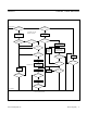
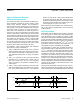
Hardware Conguration
The 1-Wire bus has only a single line by definition; it is
important that each device on the bus be able to drive
it at the appropriate time. To facilitate this, each device
attached to the 1-Wire bus must have open-drain or three-
state outputs. The 1-Wire port of the DS2431 is open drain
with an internal circuit equivalent to that shown in Figure 8.
A multidrop bus consists of a 1-Wire bus with multiple
slaves attached. The DS2431 supports both a standard
and overdrive communication speed of 15.4kbps (max)
and 125kbps (max), respectively. Note that legacy 1-Wire
products support a standard communication speed of
16.3kbps and overdrive of 142kbps. The slightly reduced
rates for the DS2431 are a result of additional recovery
times, which in turn were driven by a 1-Wire physical
interface enhancement to improve noise immunity. The
value of the pullup resistor primarily depends on the net-
work size and load conditions. The DS2431 requires a
pullup resistor of 2.2kΩ (max) at any speed.
The idle state for the 1-Wire bus is high. If for any reason
a transaction needs to be suspended, the bus must be
left in the idle state if the transaction is to resume. If this
does not occur and the bus is left low for more than 16μs
(overdrive speed) or more than 120μs (standard speed),
one or more devices on the bus could be reset.
Transaction Sequence
The protocol for accessing the DS2431 through the
1-Wire port is as follows:
● Initialization
● ROM Function Command
● Memory Function Command
● Transaction/Data
DS2431 1024-Bit, 1-Wire EEPROM
www.maximintegrated.com
Maxim Integrated
│
12