
Datasheet


DS2417
ABSOLUTE MAXIMUM RATINGS*
Voltage on 1-Wire to Ground -0.5V to +7.0V
Operating Temperature Range -40°C to +85°C
Storage Temperature Range -55°C to +125°C
Soldering Temperature See J-STD-020A Specification
* This is a stress rating only and functional operation of the device at these or any other conditions
above those indicated in the operation sections of this specification is not implied. Exposure to abso-
lute maximum rating conditions for extended periods of time may affect reliability.
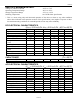
DC ELECTRICAL CHARACTERISTICS
(V
PUP
= 2.5V to 6.0V; V
DD
= 2.5V to 5.5V, -40°C to +85°C)
PARAMETER SYMBOL MIN TYP MAX UNITS NOTES
Logic 1 V
IH1
2.2 6.0 V 1, 11
Logic 0 V
IL1
-0.3 TBD V 1, 6
Output Logic Low @ 4mA V
OL1
0.4 V 1
Output Logic High V
OH1
V
PUP
V 1, 3
Input Load Current I
L1
5 µA 4
Interrupt Sink Current
@ 0.4V
I
INT3
5 mA 9
Operating Current (Osc. On) I
DD3
250 nA 2, 9
Quiescent Current (Osc. Off) I
DDQ3
50 nA 2, 8, 9
Interrupt Sink Current
@ 0.4V
I
INT5
10 mA 10
Operating Current (Osc. On) I
DD5
450 nA 2, 10
Quiescent Current (Osc. Off) I
DDQ5
100 nA 2, 8, 10
CAPACITANCE (T
A
= 25°C)
PARAMETER SYMBOL MIN TYP MAX UNITS NOTES
Capacitance 1-Wire C
IN
50 pF
AC ELECTRICAL CHARACTERISTICS
(V
PUP
= 2.5V to 6.0V; V
DD
= 2.5V to 5.5V, -40°C to +85°C)
PARAMETER SYMBOL MIN TYP MAX UNITS NOTES
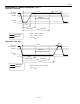
Time Slot t
SLOT
60 120 µs
Write 1 Low Time t
LOW1
1 15 µs 13
Write 0 Low Time t
LOW0
60 120 µs
Read Low Time t
LOWR
1 15 µs 13
Read Data Valid t
RDV
15 µs 12
Release Time t
RELEASE
0 15 45 µs
Read Data Setup t
SU
1 µs 5
Recovery Time t
REC
1 µs
Reset High Time t
RSTH
480 µs
Reset Low Time t
RSTL
480 960 µs 7
Presence Detect High t
PDH
15 60 µs
Presence Detect Low t
PDL
60 240 µs
14 of 15