
Datasheet


DS1992/DS1993
13 of 17
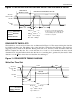
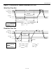
Figure 10. INITIALIZATION PROCEDURE RESET AND PRESENCE PULSE
RESISTOR
MASTER
DS199x
MASTER RX "PRESENCE PULSE"
480 µs
≤
t
RSTL
<
∞
*
480 µs
≤
t
RSTH
<
∞
**
15 µs
≤
t
PDH
< 60 µs
60
≤
t
PDL
< 240 µs
MASTER T
X
"RESET PULSE"
V
PULLUP
V
PULLUP MIN
V
IH MIN
V
IL MAX
0V
t
RSTH
t
RSTL
t
PDH
t
PDL
t
R
* In order not to mask interrup signaling
by other devices on the 10Wire bus t
RSTL
+ t
R
should always be less than 960 us
** Includes recovery time
READ/WRITE TIME SLOTS
The definitions of write and read time slots are illustrated in Figure 11. The master driving the data line
low initiates all time slots. The falling edge of the data line synchronizes the DS199x to the master by
triggering a delay circuit in the DS199x. During write time slots, the delay circuit determines when the
DS199x samples the data line. For a read data time slot, if a 0 is to be transmitted, the delay circuit
determines how long the DS199x holds the data line low overriding the 1 generated by the master. If the
data bit is a 1, the iButton leaves the read data time slot unchanged.
Figure 11. READ/WRITE TIMING DIAGRAM
Write-One Time Slot
15µs
60µs
DS199x
Sampling Window
V
PULLUP
V
PULLUP MIN
V
IH MIN
V
IL MAX
0V
t
SLOT
t
REC
t
LOW1
60 µs
≤
t
SLOT
< 120 µs
1 µs
≤
t
LOW1
< 15 µs
1 µs
≤
t
REC
<
∞
RESISTOR
MASTER