
Datasheet


DS1982
Page 7 of 24
MEMORY FUNCTION COMMANDS
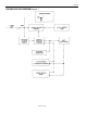
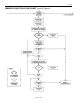
The “Memory Function Flow Chart” (Figure 6) describes the protocols necessary for accessing the
various data fields within the DS1982. The Memory Function Control section, 8-bit scratchpad, and the
Program Voltage Detect circuit combine to interpret the commands issued by the bus master and create
the correct control signals within the device. A 3-byte protocol is issued by the bus master. It is comprised
of a command byte to determine the type of operation and 2 address bytes to determine the specific
starting byte location within a data field. The command byte indicates if the device is to be read or
written. Writing data involves not only issuing the correct command sequence but also providing a 12-
volt programming voltage at the appropriate times. To execute a write sequence, a byte of data is first
loaded into the scratchpad and then programmed into the selected address. Write sequences always occur
a byte at a time. To execute a read sequence, the starting address is issued by the bus master and data is
read from the part beginning at that initial location and continuing to the end of the selected data field or
until a reset sequence is issued. All bits transferred to the DS1982 and received back by the bus master
are sent least significant bit first.
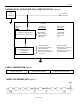
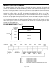
DS1982 MEMORY MAP Figure 5
PAGE 0
32 BYTES
PAGE 1
32 BYTES
PAGE 2
32 BYTES
PAGE 3
32 BYTES
EPROM STATUS BYTES
ADDRESS: 0007h 0006h 0005h 0004h 0003h 0002h 0001h 0000h
(MSB) (LSB)
BIT 0 WRITE PROTECT PAGE 0
BIT 1 WRITE PROTECT PAGE 1
BIT 2 WRITE PROTECT PAGE 2
BIT 3 WRITE PROTECT PAGE 3
BIT 4-7 BITMAP OF USED PAGES (RESERVED FOR TMEX)
8-BIT SCRATCHPAD
1024-BIT
EPROM
STARTING
ADDRESS
0000h
00
2
0
h
0040h
0060h