
Datasheet


DS1882
Dual Log Audio Digital Potentiometer
6 _____________________________________________________________________
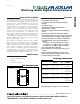
DECODER
POTENTIOMETER 0
VALUE
CONFIGURATION
REGISTER
POTENTIOMETER
SETTING
REGISTERS
GND
ZERO-CROSSING
DETECTOR
H0
W0
L0
UPDATE UPDATE
H1
W1
L1
I
2
C
INTERFACE
SDA
SCL
A2
A0
A1
CE
V
CC
V
CC
V
DD
V
DD
GND
ZERO-CROSSING
DETECTOR
POTENTIOMETER 1
VALUE
V-
V-
DS1882
Block Diagram
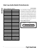
Pin Description
PIN NAME FUNCTION
1 GND Ground
2A2
3A1
I
2
C Address Inputs. Inputs A0, A1, and A2 determine the I
2
C slave address of the device.
4 V- Negative Analog Voltage Supply
5A0I
2
C Address Input. Inputs A0, A1, and A2 determine the I
2
C slave address of the device.
6 W0 Wiper Terminal for Potentiometer 0
7 L0 Low Terminal for Potentiometer 0
8 H0 High Terminal for Potentiometer 0
9 L1 Low Terminal for Potentiometer 1
10 H1 High Terminal for Potentiometer 1
11 W1 Wiper Terminal for Potentiometer 1
12 CE Chip Enable. Enables SDA and SCL pins for I
2
C communication.
13 SDA I
2
C Serial-Data Open-Drain I/O
14 SCL I
2
C Serial-Clock Input
15 V
CC
Analog Voltage Supply
16 V
DD
Digital Voltage Supply