
Datasheet


DS1881
Dual NV Audio Taper Digital Potentiometer
4 _____________________________________________________________________
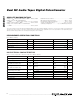
NV MEMORY CHARACTERISTICS
(V
DD
= +2.7V to +5.5V, V
CC
= +4.5V to +5.5V, T
A
= 0°C to +70°C.)
PARAMETER
SYMBOL
CONDITIONS MIN
TYP MAX
UNITS
Writes +70°C (Note 6)
50,000
Note 1: All voltages are referenced to ground.
Note 2: The value of V
DD
should never exceed V
CC
, including during power-ups. V
CC
must be applied before V
DD
.
Note 3: I
DD
is specified with SDA = SCL = CE = V
DD
, resistor pins floating, and digital inputs connected to V
DD
or GND.
Note 4: I
CC
is specified with SDA = SCL = CE = V
DD
, resistor pins floating, and digital inputs connected to V
DD
or GND, after zero-
crossing detection has timed out.
Note 5: The DS1881 will not obstruct the SDA and SCL lines if V
DD
is switched off as long as the voltages applied to these inputs
do not violate their minimum and maximum input voltage levels.
Note 6: Guaranteed by design.
Note 7: Above Position 50, these are typical maximum. Guaranteed by characterization.
Note 8: Load is representative of the input of a low-noise audio amp.
Note 9: Timing shown is for fast-mode (400kHz) operation. This device is also backward-compatible with I
2
C standard-mode timing.
Note 10: C
B
—Total capacitance of one bus line in picofarads.
Note 11: If zero-crossing detection is enabled, the EEPROM write does not begin until the current zero-crossing detection is com-
plete. Otherwise, EEPROM write begins after a STOP condition occurs.
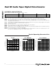
I
DD
vs. V
DD
DS1881 toc01
VOLTAGE (V)
SUPPLY CURRENT (µA)
5.35.14.7 4.9
120
140
160
180
200
220
240
260
280
300
100
4.5 5.5
SDA = SCL = V
CC
I
DD
vs. TEMPERATURE
DS1881 toc02
TEMPERATURE (°C)
SUPPLY CURRENT (µA)
8060-20 0 20 40
50
100
150
200
250
300
350
400
0
-40
SDA = SCL = V
DD
I
DD
vs. SCL FREQUENCY
DS1881 toc03
SCL FREQUENCY (kHz)
ACTIVE SUPPLY CURRENT (µA)
400300 35025050 100 150 200
50
100
150
200
250
300
350
400
0
0
SDA = V
DD
Typical Operating Characteristics
(V
DD
= V
CC
= +5.0V, T
A
= +25°C.)