
Datasheet


DS1881
Dual NV Audio Taper Digital Potentiometer
2 _____________________________________________________________________
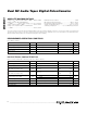
ABSOLUTE MAXIMUM RATINGS
RECOMMENDED OPERATING CONDITIONS
(T
A
= -40°C to +85°C)
Stresses beyond those listed under “Absolute Maximum Ratings” may cause permanent damage to the device. These are stress ratings only, and functional
operation of the device at these or any other conditions beyond those indicated in the operational sections of the specifications is not implied. Exposure to
absolute maximum rating conditions for extended periods may affect device reliability.
Voltage on V
DD
, SDA, and SCL Relative to GND .....-0.5V to +6.0V
Voltage on A2, A1, A0, and
CE Relative
to GND .................-0.5V to (V
DD
+ 0.5V), not to exceed +6.0V
Voltage on V
CC
Relative to GND...........................-0.5V to +6.0V
Voltage on H1, H0, W1, W0, L1, and L0 Relative
to GND...............................................................-0.5V to +6.0V
Maximum Resistor Current .................................................±3mA
Operating Temperature Range ...........................-40°C to +85°C
Programming Temperature Range .........................0°C to +70°C
Storage Temperature Range .............................-55°C to +125°C
Soldering Temperature...................See J-STD-020 Specification
PARAMETER
SYMBOL
CONDITIONS MIN
TYP MAX
UNITS
Digital Supply Voltage
V
DD
(Notes 1, 2) 2.7 5.5 V
Analog Supply Range
V
CC
(Notes 1, 2) 4.5 5.5 V
Potentiometer Voltages
0 5.5 V
Wiper Current ±1 mA
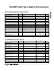
DC ELECTRICAL CHARACTERISTICS
(V
DD
= +2.7V to +5.5V, V
CC
= +4.5V to +5.5V, T
A
= -40°C to +85°C.)
PARAMETER
SYMBOL
CONDITIONS MIN
TYP MAX
UNITS
Digital Supply Current I
DD
(Note 3) 200 250 µA
Analog Supply Current I
CC
(Note 4) 0.9 5 µA
Input Logic 0
(CE, SDA, SCL, A0, A1, A2)
V
IL
(Note 5) -0.3
0.3x
V
DD
V
Input Logic 1
(CE, SDA, SCL, A0, A1, A2)
V
IH
(Note 5)
0.7 x
V
DD
V
DD
+
0.3
V
I
OL
= 4mA 0.4
Output-Voltage Low (SDA) V
OL
I
OL
= 6mA 0.6
V
Input Leakage Current I
LI
-1 +1 µA
I/O Pin Input Current (SDA) 0.4V < V
SDA
< (0.9 x V
CC
) -10 +10 µA
I/O Capacitance C
I/O
(Note 6) 10 pF
Power-Up Time t
PU
1ms