
Datasheet


DS1846
2 of 18
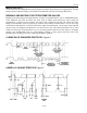
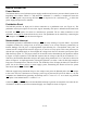
The EEPROM memory allows a user to store configuration or calibration data for a specific system or
device and provides control of the potentiometer wiper settings. Any type of user information can reside
in the first 248 bytes (00h to F7h) of this memory. The next three bytes of memory (F8h to FAh) are for
potentiometer settings and the last five addresses of EEPROM memory (FBh to FFh) are reserved. These
reserved and potentiometer registers should not be used for data storage. Access to this EEPROM is
through an industry-standard 2-wire bus. The interface I/O pins consist of SDA and SCL. The wiper
positions of the DS1846, as well as EEPROM data, can be hardware write-protected using the WP input
pin.
The MicroMonitor is a precision temperature-compensated reference and comparator that monitors
certain vital status conditions for a microprocessor. When a sense input detects an out-of-tolerance (V
CC
)
condition, a nonmaskable interrupt is generated. As the voltage at the device degrades, an internal power-
fail signal is generated that can be used to reset the processor. When V
CC
returns to an in-tolerance level,
the reset signal is kept in the active state for a minimum time of t
RST
to allow for the stabilization of the
power supply and the microprocessor. The MicroMonitor also functions as a pushbutton reset control.
The pushbutton input is debounced internally and generates an active pulse width of t
RST
minimum.
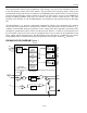
DS1846 BLOCK DIAGRAM Figure 1
DS1846
2-Wire
Interface
SCL
SDA
WP
A
0
5 Reserved
Bytes
FBh-FFh
Potentiometer 2
FAh
Potentiometer 0
F9h
Potentiometer 1
F8h
User EPROM
248 Bytes
00h-F7h
EEPROM
Potentiometer 2
H2
W2
L2
10kW
A
ddr FAh
100-Positions
Potentiometer 0
H0
W0
L0
10kW
A
ddr F9h
100-Positions
Potentiometer 1
H1
W1
L1
100kW
A
ddr F8h
256-Positions
Data
Nonvolatile
Digital Potentiometer
PBRST
V
CCTP
V
TP
V
CC
IN
RST
RST
V
CC
NMI
MicroMonitor
Timer
Delay
Timer
Delay
V
CC
2.4kW
typical
R
PBR