
Datasheet


DS1846
18 of 18
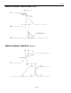
NOTES:
1) All voltages are referenced to ground.
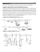
2) I/O pins of fast-mode devices must not obstruct the SDA and SCL lines if V
CC
is switched off.
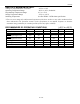
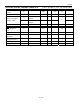
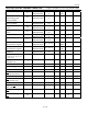
3) I
STBY
specified with V
CC
= 5.0V and control port logic pins are driven to the appropriate logic levels.
Appropriate logic levels specify that logic inputs are within a 0.5V of ground or V
CC
for the
corresponding inactive state. All inputs should be connected high.
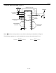
4) A fast-mode device can be used in a standard mode system, but the requirement t
SU:DAT
> 250ns must
then be met. This is automatically the case if the device does not stretch the low period of the SCL
signal. If such a device does stretch the low period of the SCL signal, it must output the next data bit
to the SDA line t
RMAX
+ t
SU:DAT
= 1000ns + 250ns = 1250ns before the SCL line is released.
5) After this period, the first clock pulse is generated.
6) The maximum t
HD:DAT
has only to be met if the device does not stretch the low period (t
LOW
) of the
SCL signal.
7) A device must internally provide a hold time of at least 300ns for the SDA signal (referred to the V
IN
MIN
of the SCL signal) to bridge the undefined region of the falling edge of SCL.
8) C
B
—total capacitance of one bus line in picofarads, timing referenced to (0.9 x V
CC
) and (0.1 x V
CC
).
9) EEPROM write begins after a stop condition occurs.
10) Resistor inputs can not go beneath GND by more than 0.5V or above V
CC
by more than 0.5V.
11) Absolute linearity is used to measure expected wiper voltage as determined by wiper position.
12) Relative linearity is used to determine the change of wiper voltage between two adjacent wiper
positions.
13) When used as a rheostat or variable resistor the temperature coefficient applies: 750ppm/°C. When
used as a voltage-divider or potentiometer, the effective temperature coefficient approaches
30ppm/°C.
14) Valid for V
CC
= 5V only.
15) Valid at +25°C only.
16) Noise immunity pulses < 2ms at V
CCTP
minimum do not cause a reset.