
Datasheet
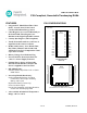

DS1747/DS1747P Y2K-Compliant, Nonvolatile Timekeeping RAMs
8 of 16
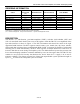
ABSOLUTE MAXIMUM RATINGS
Voltage Range on Any Pin Relative to Ground
5.5V Version………………………………………………………………………………………….-0.3V to +6.0V
3.3V Version.…………………………………………………………………………………………-0.3V to +4.6V
Operating Temperature Range (Noncondensing)
Commercial...……………………………………….......................................................................0°C to +70°C
Industrial……………………………………………………..……………………………………….-40°C to +85°C
Storage Temperature Range
EDIP .......................………………………………………………………………………………...-40°C to +85°C
PowerCap ........................................................................................................................... -55°C to +125°C
Lead Temperature (soldering, 10s)..........................……………………….………….…………………………...+260°C
Note: EDIP is hand or wave-soldered only.
Soldering Temperature (reflow, PowerCap) .................................................................................................. +260°C
This is a stress rating only and functional operation of the device at these or any other condition above those indicated in the operation
sections of this specification is not implied. Exposure to absolute maximum rating conditions for extended periods of time may affect device
reliability.
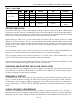
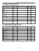
RECOMMENDED DC OPERATING CONDITIONS
(T
A
= Over the Operating Range)
PARAMETER SYMBOL MIN TYP MAX UNITS NOTES
Logic 1 Voltage
All Inputs
V
CC
=
5V±10%
V
IH
2.2
V
CC
+
0.3V
V 1
V
CC
=
3.3V±10%
V
IH
2.0
V
CC
+
0.3V
V 1
Logic 0 Voltage
All Inputs
V
CC
=
5V±10%
V
IL
-0.3 +0.8 V 1
V
CC
=
3.3V±10%
V
IL
-0.3 +0.6 V 1
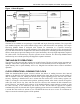
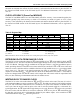
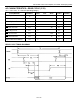
DC ELECTRICAL CHARACTERISTICS
(V
CC
= 5.0V ± 10%, T
A
= Over the Operating Range.)
PARAMETER SYMBOL MIN TYP MAX UNITS NOTES
Active Supply Current
Icc
85
mA
2, 3, 10
TTL Standby Current
(
CE
= V
IH
)
Icc
1
6 mA 2, 3
CMOS Standby Current
(
CE
≥ V
CC
- 0.2V)
Icc
2
4 mA 2, 3
Input Leakage Current
(Any Input)
I
IL
-1 +1
µA
Output Leakage Current
(Any Output)
I
OL
-1 +1
µA
Output Logic 1 Voltage
(I
OUT
= -1.0mA)
V
OH
2.4 1
Output Logic 0 Voltage
(I
OUT
= +2.1mA)
V
OL
0.4 1
Write Protection Voltage V
PF
4.25 4.50 V 1
Battery Switchover Voltage V
SO
V
BAT
1, 4