
Datasheet


DS1743/DS1743P Y2K-Compliant, Nonvolatile Timekeeping RAMs
7 of 17
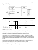
Table 2. Register Map
ADDRESS
DATA
FUNCTION RANGE
B
7
B
6
B
5
B
4
B
3
B
2
B
1
B
0
1FFF
10 Year
Year
Year
00–99
1FFE X X X
10
Month
Month Month 01–12
1FFD
X
X
10 Date
Date
Date
01–31
1FFC
BF
FT
X
X
X
Day
Day
01–07
1FFB
X
X
10 Hour
Hour
Hour
00–23
1FFA
X
10 Minutes
Minutes
Minutes
00–59
1FF9
OSC
10 Seconds
Seconds
Seconds
00–59
1FF8
W
R
10 Century
Century
Control
00–39
OSC = STOP BIT
R = READ BIT
FT = FREQUENCY TEST
W = WRITE BIT
X = SEE NOTE BELOW
BF = BATTERY FLAG
Note: All indicated “X” bits must be set to “0” when written to ensure proper clock operation.
RETRIEVING DATA FROM RAM OR CLOCK
The DS1743 is in the read mode whenever OE (output enable) is low, WE (write enable) is high, and CE
(chip enable) is low. The device architecture allows ripple-through access to any of the address locations in
the NV SRAM. Valid data will be available at the DQ pins within t
AA
after the last address input is stable,
providing that the, CE and OE access times and states are satisfied. If CE, or OE access times and states
are not met, valid data will be available at the latter of chip enable access (t
CEA
) or at output enable access
time (t
CEA
). The state of the data input/output pins (DQ) is controlled by CE and OE. If the outputs are
activated before t
AA
, the data lines are driven to an intermediate state until t
AA
. If the address inputs are
changed while CE and OE remain valid, output data will remain valid for output data hold time (t
OH
) but
will then go indeterminate until the next address access.