
Datasheet


DS1743/DS1743P Y2K-Compliant, Nonvolatile Timekeeping RAMs
5 of 17
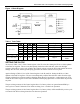
Figure 1. Block Diagram
Table 1. Truth Table
V
CC
CE
CE2
OE
WE
MODE
DQ
POWER
V
CC
> V
PF
V
IH
X
X
X
Deselect
High-Z
Standby
X
V
IL
X
X
Deselect
High-Z
Standby
V
IL
V
IH
X
V
IL
Write
Data In
Active
V
IL
V
IH
V
IL
V
IH
Read
Data Out
Active
V
IL
V
IH
V
IH
V
IH
Read
High-Z
Active
V
SO
< V
CC
< V
PF
X
X
X
X
Deselect
High-Z
CMOS Standby
V
CC
<V
SO
<V
PF
X X X X Deselect High-Z
Data-Retention
Mode
SETTING THE CLOCK
As shown in Table 2, bit 7 of the Control register is the W (write) bit. Setting the W bit to 1 halts updates
to the DS1743 registers. The user can subsequently load correct date and time values into all eight
registers, followed by a write cycle of 00h to the Control register to clear the W bit and transfer those new
settings into the clock, allowing timekeeping operations to resume from the new set-point.
Again referring to Table 2, bit 6 of the Control register is the R (read) bit. Setting the R bit to 1 halts
updates to the DS1743 registers. The user can subsequently read the date and time values from the eight
registers without those contents possibly changing during those I/O operations. A subsequent write cycle
of 00h to the Control register to clear the R bit allows timekeeping operations to resume from the previous
set-point.
The pre-existing contents of the Control register bits 0:5 (Century value) are ignored/unmodified by a
write cycle to Control if either the W or R bits are being set to 1 in that write operation.
The pre-existing contents of the Control register bits 0:5 (Century value) will be modified by a write cycle
to Control if the W bit is being cleared to 0 in that write operation.
Dallas
Semiconductor
DS1743