
Datasheet


DS17285/DS17287/DS17485/DS17487/DS17885/DS17887
Real-Time Clocks
_____________________________________________________________________
7
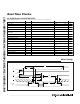
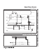
SUPPLY CURRENT
vs. INPUT VOLTAGE
DS17285/87 toc01
V
BAT
(V)
SUPPLY CURRENT (nA)
3.53.33.02.8
250
300
350
400
200
2.5 3.8
V
CC
= 0V
SUPPLY CURRENT
vs. TEMPERATURE
DS17285/87 toc02
TEMPERATURE (°C)
SUPPLY CURRENT (nA)
65503520
5
-10-25
300
350
400
250
-40 80
V
BAT
= 3.0V
OSCILLATOR FREQUENCY
vs. SUPPLY VOLTAGE
DS17285/87 toc03
SUPPLY VOLTAGE (V)
OSCILLATOR FREQUENCY (Hz)
5.04.54.03.53.0
32768.1
32768.2
32768.3
32768.4
32768.5
32768.6
32768.7
32768.0
2.5 5.5
Typical Operating Characteristics
(V
CC
= +3.3V, T
A
= +25°C, unless otherwise noted.)
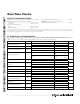
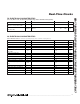
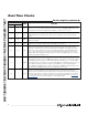
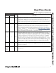
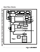
Pin Description
PIN
24 28
NAME FUNCTION
1 8 PWR
Active-Low Power-On Reset. This open-drain output pin is intended for use as an on/off
control for the system power. With V
CC
voltage removed from the device, PWR can be
automatically activated from a kickstart input by the KS pin or from a wake-up interrupt.
Once the system is powered on, the state of PWR can be controlled by bits in the control
registers. The PWR pin can be connected through a pullup resistor to a positive supply. For
5V operation, the voltage of the pullup supply should be no greater than 5.7V. For 3V
operation, the voltage on the pullup supply should be no greater than 3.9V.
2, 3 9, 10 X1, X2
Connections for Standard 32.768kHz Quartz Crystal. The internal oscillator circuitry is
designed for operation with a crystal having a specified load capacitance (C
L
) of 6pF or
12.5pF. Pin X1 is the input to the oscillator and can optionally be connected to an external
32.768kHz oscillator. The output of the internal oscillator, pin X2, is left unconnected if an
external oscillator is connected to pin X1. These pins are missing (N.C.) on the EDIP
package.
4–11
12–17,
19, 20
AD0–AD7
Multiplexed Bidirectional Address/Data Bus. The addresses are presented during the first
portion of the bus cycle and latched into the device by the falling edge of ALE. Write data is
latched by the rising edge of WR. In a read cycle, the device outputs data during the latter
portion of the RD low. The read cycle is terminated and the bus returns to a high-impedance
state as RD transitions high.
12, 16 21, 22, 26 GND Ground