
Datasheet


DS1685/DS1687 3V/5V Real-Time Clocks
5 of 34
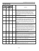
PIN DESCRIPTIONS (continued)
PIN
NAME
FUNCTION
DS1685 DS1687
PDIP,
SO,
TSSOP
PLCC EDIP
18 22 18
KS
Kickstart Input, Active Low. When V
CC
is removed from the
DS1685/DS1687, the system can be powered on in response to an active-
low transition on the KS pin, as might be generated from a key closure.
V
BAUX
must be present and the auxiliary-battery enable bit (ABE) and kick-
start enable bit (KSE) must be set to 1 if the kickstart function is used, and
the KS pin must be pulled up to the V
BAUX
supply. While V
CC
is applied, the
KS pin can be used as an interrupt input. If not used, connect to V
CC
, or to
V
BAUX
if V
BAUX
is used.
19 23 19
IRQ
Interrupt-Request Output, Open Drain, Active Low. The IRQ pin is an
active-low output of the DS1685/DS1687 that can be connected to the
interrupt input of a processor. The IRQ output remains low as long as the
status bit causing the interrupt is present and the corresponding interrupt-
enable bit is set. To clear the IRQ pin, the application software must clear
all the enabled flag bits contributing to IRQ’s active state asserted but
without asserting CS latch addresses. However, no data transfer occurs.
20 24 — V
BAT
Battery Input for Any Standard 3V Lithium Cell or Other Energy Source.
Battery voltage must be held between 2.5V and 3.7V for proper operation.
V
BAT
must be grounded if not used. Diodes should not be placed between
V
BAT
and the battery. See “Conditions of Acceptability” at
www.maximintegrated.com/UL
.
21 25 21
RCLR
RAM Clear Input, Active Low. If enabled by software, taking RCLR low
clears the 242 bytes of user RAM to FFh. When enabled, RCLR can be
activated whether or not V
CC
is present. The RCLR function is designed to
be used by a human interface (shorting to ground manually or by a switch)
and not to be driven with external buffers. This pin is internally pulled up.
Do not use an external pullup resistor on this pin.
22 26 22 V
BAUX
Auxiliary Battery Input. Required for kickstart and wake-up features. This
input also supports clock/ calendar and user RAM if V
BAT
is at lower voltage
or is not present. A standard +3V lithium cell or other energy source can be
used. Battery voltage must be held between +2.5V and +3.7V for proper
operation. If V
BAUX
is not going to be used it should be grounded, and
Auxiliary-Battery Enable bit bank 1, register 4BH, should be written to 0.
See “Conditions of Acceptability” at www.maximintegrated.com/UL
.
23 27 23 SQW
Square-Wave Output. The SQW pin provides a 32kHz square-wave output,
t
REC
, after a power-up condition has been detected. This condition sets the
following bits, enabling the 32kHz output; DV1 = 1, and E32K = 1. A square
wave is output on this pin if either SQWE = 1 or E32K = 1. If E32K = 1, then
32kHz is output regardless of the other control bits. If E32K = 0, then the
output frequency is dependent on the control bits in register A. The SQW
pin can output a signal from one of 13 taps provided by the 15 internal
divider stages of the RTC. The frequency of the SQW pin can be changed
by programming Register A as shown in Table 3. The SQW signal can be
turned on and off using the SQWE bit in register B or the E32K bit in
extended register 4Bh. A 32kHz SQW signal is output when the enable-
32kHz (E32K) bit in extended register 4Bh is a logic 1 and V
CC
is above
V
PF
. A 32kHz square wave is also available when V
CC
is less than V
PF
if
E32K = 1, ABE = 1, and voltage is applied to the V
BAUX
pin.
24 28 24 V
CC
DC Power for Primary Power Supply. When V
CC
is applied within the
normal limits, the device sis fully accessible and data can be written and
read. When V
CC
is below V
PF
reads and writes are inhibited.