
Datasheet

DS1685/DS1687 3V/5V Real-Time Clocks
22 of 34
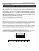
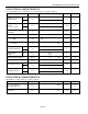
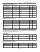
Extended Control Register 4B
MSB
LSB
BIT 7
BIT 6
BIT 5
BIT 4
BIT 3
BIT 2
BIT 1
BIT 0
ABE
E32K
CS
RCE
PRS
RIE
WIE
KSE
ABE – Auxiliary Battery Enable. This bit when written to a logic 1 enables the V
BAUX
pin for extended functions.
E32K – Enable 32.768kHz output. This bit when written to a logic 1 enables the 32.768kHz oscillator frequency to
be output on the SQW pin. This bit is set to a logic 1 when V
CC
is applied.
CS – Crystal Select Bit. When CS is set to a 0, the oscillator is configured for operation with a crystal that has a
6pF specified load capacitance. When CS = 1, the oscillator is configured for a 12.5pF crystal. CS is disabled in the
DS1687 EDIP and should be set to CS = 0.
RCE – RAM Clear-Enable bit. When set to a 1, this bit enables a low level on RCLR to clear all 242 bytes of user
RAM. When RCE = 0, RCLR and the RAM clear function are disabled.
PRS – PAB Reset-Select Bit. When set to a 0, the PWR pin is set high-Z when the DS1685 goes into power-fail.
When set to a 1, the PWR pin remains active upon entering power-fail.
RIE – Ram Clear-Interrupt Enable. When RIE is set to a 1, the IRQ pin is driven low when a RAM clear function is
completed.
WIE – Wake-Up Alarm-Interrupt Enable. When V
CC
voltage is absent and WIE is set to a 1, the PWR pin is driven
active-low when a wake-up condition occurs, causing the WF bit to be set to 1. When V
CC
is then applied, the IRQ
pin is also driven low. If WIE is set while system power is applied, both IRQ and PWR are driven low in response to
WF being set to 1. When WIE is cleared to a 0, the WF bit has no affect on the PWR or IRQ pins.
KSE – Kickstart Interrupt Enable. When V
CC
voltage is absent and KSE is set to a 1, the PWR pin is driven active-
low when a kickstart condition occurs (KS pulsed low), causing the KF bit to be set to 1. When V
CC
is then applied,
the IRQ pin is also driven low. If KSE is set to 1 while system power is applied, both IRQ and PWR are driven low in
response to KF being set to 1. When KSE is cleared to a 0, the KF bit has no affect on the PWR or IRQ pins.
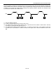
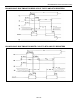
SYSTEM MAINTENANCE INTERRUPT (SMI) RECOVERY STACK
An SMI recovery register stack is located in the extended register bank, locations 4Eh and 4Fh. This register stack,
shown below, can be used by the BIOS to recover from an SMI occurring during an RTC read or write.
RTC ADDRESS
RTC ADDRESS-1
4Eh RTC ADDRESS-2
4Fh RTC ADDRESS-3
SMI RECOVERY STACK
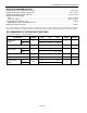
7 6 5 4 3 2 1 0
DV0 AD6 AD5 AD4 AD3 AD2 AD1 AD0
REGISTER BIT DEFINITION