
Datasheet
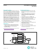


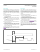


Figure 2. Total Run Time
DS1682
V
CC
EVENT
TRIGGER SWITCH
LED
SCL
PUSHBUTTON
SWITCH
ALARM
SDAGND
0.01µF
Operation
The block diagram in Figure 1 shows the relationship
between the major functional blocks, the serial interface,
and the EEPROM memory section of the DS1682. Upon
power-up, the DS1682 transfers the contents of the
EEPROM into the counters and memory registers where
the data can be read and written through the serial inter-
face. The content of the counters and memory registers
are written into the EEPROM memory when the EVENT
pin transitions from a logic-high to a logic-low.
The DS1682 uses a calibrated, temperature-compensat-
ed RC time base to increment an ETC while an event
is active. When the event becomes active, the contents
of the nonvolatile EEPROM are transferred to the ETC
and event counter and the oscillator starts. As the event
continues, the ETC is incremented in quarter-second
increments. When the event becomes inactive, the event
counter is incremented and the contents of the ETC and
event counter are written to the nonvolatile EEPROM.
The ALARM output can be used to indicate when the ETC
has matched the value in the alarm register.
The DS1682 can be configured to prevent clearing the
alarm and the elapsed time and event counters.The user
memory can be separately write protected.
User-modified data is not stored in EEPROM until an
event becomes inactive.
Figure 2 shows the DS1682 measuring total run time and
operating from a battery with the alarm tied to an LED and
a pushbutton switch to trigger the alarm output.
Figure 3 shows the DS1682 in a total time-of-use applica-
tion where power may be removed at the same time as
the end of the event. The V
CC
slew rate at power-down is
fast with respect to t
EW
. A capacitor maintains V
CC
on the
DS1682 above 2.5V until the EEPROM write completes. A
Schottky diode blocks current from the capacitor to other
devices connected to V
CC
.
The V
CC
holding capacitor value of 30μF is calculated
using the maximum EEPROM write current and EEPROM
write time. This assumes that the V
CC
slew rate allows
time from EVENT trip point to V
CC
at 2.5V on the DS1682
is at least t
EW
.
Figure 4 shows the DS1682 in a total time-of-use applica-
tion with power that can be removed at the sametime as
the end of the event. In this application, the V
CC
slew rate
at power-down is slow with respect to t
EW
. The external
reset IC (DS1816) ends the event as V
CC
begins to drop.
V
CC
must remain above 2.5V until the end of t
EW
.
Figure 3. Total Time-of-Use Application with Fast V
CC
Slew Rate
DS1682
V
CC
EVENT
LED
SCLALARM
SDAGND
0.01µF 30µF typ
V
CC
Figure 4. Total Time-of-Use Application with Slow V
CC
Slew Rate
DS1682
V
CC
ALARM
LED
SCLEVENT
SDAGND
0.01µF
R
PU
= t
R
/C
BUS
R
PU
R
PU
V
CC
V
CC
DS1816
DS1682 Total-Elapsed-Time Recorder
with Alarm
www.maximintegrated.com
Maxim Integrated
│
6