
Datasheet


Note 1: Typical values are at T
A
= +25°C, V
CC
= 4.0V.
Note 2: The elapsed time and event counters are backed by three EEPROM arrays, which are used sequentially, allowing up to 3 x
E
E
. The configuration register, alarm trip-point register, and user memory use a single array, limiting them to one E
E
.
Note 3: A decoupling capacitor to supply high instantaneous currents during EEPROM writes is recommended. A typical value is
0.01μF. V
CC
must be maintained above V
CC
minimum, including transients, during EEPROM writes.
Note 4: VCC must be at or above 2.5V for t
EW
after the end of an event to ensure data transfer to the EEPROM.
Note 5: Reading data while the contents of EEPROM are transferred to RAM results in incorrect reads.
Note 6: After this period, the first clock pulse is generated.
Note 7: A device must internally provide a hold time of at least 300ns for the SDA signal (referred to the V
IH(MIN)
of the SCL signal)
to bridge the undefined region of the falling edge of SCL.
Note 8: The maximum t
HD:DAT
has only to be met if the device does not stretch the low period (t
LOW
) of the SCL signal.
Note 9: A fast-mode device can be used in a standard-mode system, but the requirement t
SU:DAT
≥ 250ns must be met. This is
automatically the case if the device does not stretch the t
LOW
. If such a device does stretch t
LOW
, it must output the next
data bit to the SDA line t
R(MAX)
+ t
SU:DAT
= 1000 + 250 = 1250ns before the SCL line is released.
Note 10:
C
B
—Total capacitance of one bus line in pF.
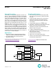
SCL
NOTE: TIMING IS REFERENCED TO V
IL(MAX)
AND V
IH(MIN)
.
SDA
STOP START REPEATED
START
t
BUF
t
HD:STA
t
HD:DAT
t
SU:DAT
t
SU:STO
t
HD:STA
t
SP
t
SU:STA
t
HIGH
t
R
t
F
t
LOW
DS1682 Total-Elapsed-Time Recorder
with Alarm
www.maximintegrated.com
Maxim Integrated
│
4
Timing Diagram