
Datasheet


DS1677
7 of 18
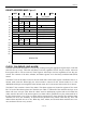
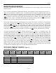
STATUS REGISTER
BIT 7 BIT 6 BIT 5 BIT 4 BIT 3 BIT 2 BIT 1 BIT 0
CU LOBAT 0 0 0 0 0 IRQF
CU (Conversion Update In Progress). When this bit is a one, an update to the ADC Register (register
0Eh) will occur within 488 μs. When this bit is a zero, an update to the ADC Register will not occur for at
least 244 μs.
LOBAT (Low Battery Flag). This bit reflects the status of the backup power source connected to the
V
BAT
pin. When V
BAT
is greater than 2.5V, LOBAT is set to a logic 0. When V
BAT
is less than 2.3V,
LOBAT is set to a logic 1.
IRQF (Interrupt Request Flag). A logic 1 in the Interrupt Request Flag bit indicates that the current
time has matched the time of day Alarm registers. If the AIE bit is also a logic 1, the INT pin will go
high. IRQF is cleared by reading or writing to any of the alarm registers.
POWER-UP DEFAULT STATES
These bits are set to a one upon initial power-up: EOSC , TD0 and TD1. These bits are cleared upon
initial power-up: WP, AIS1, and AIS0.
NONVOLATILE SRAM CONTROLLER
The DS1677 provides automatic backup and write protection for an external SRAM. This function is
provided by gating the chip enable signal and by providing a constant power supply through the V
CCO
pin.
The DS1677 nonvolatizes the external SRAM by write protecting the SRAM and by providing a back–up
power supply in the absence of V
CC
. When V
CC
falls below V
PF
, access to the external SRAM is
prohibited by forcing CE0 high regardless of the level of CEI . Upon power-up, access is prohibited until
the end of t
RPU
.
POWER-FAIL COMPARATOR
The PFI input is connected to an internal reference. If PFI is less than 1.25V, PFO goes low. The power-
fail comparator can be used as an undervoltage detector to signal an impending power supply failure.
PFO can be used as a P interrupt input to prepare for power-down. For battery conservation, the
comparator is turned off and PFO is held low when in battery-backed mode
ADDING HYSTERESIS TO THE POWER-FAIL COMPARATOR
Hysteresis adds a noise margin to the power-fail comparator and prevents PFO from oscillating when V
IN
is near the power-fail comparator trip point. Figure 8 shows how to add hysteresis to the power-fail
comparator. Select the ratio of R1 and R2 such that PFI sees 1.25V when V
IN
falls to the desired trip point
(V
TRIP
). Resistors R2 and R3 add hysteresis. R3 will typically be an order of magnitude greater than R1 or
R2. R3 should be chosen in manner to prevent it from loading down the PFO pin. Capacitor C1 adds
noise filtering and has a value of typically 1.0F. See Figure 8 for a schematic diagram and equations.