
Datasheet


DS1677
17 of 18
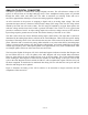
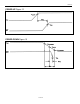
POWER-FAIL WARNING Figure 14
NOTES:
1. All voltages are referenced to ground.
2. I
CCA
is specified with outputs open, CS set to a logic 1, SCLK = 500kHz, oscillator enabled, and ADC
enabled.
3. I
ADC
is specified with CS, V
CCO
open and I/O, SCLK at logic 0. ADC is enabled.
4. I
CCS
is specified with CS, V
CCO
open and I/O, SCLK at logic 0. ADC is disabled.
5. CS has a 40k pulldown resistor to ground.
6. Measured at V
IH
= 2.0V or V
IL
= 0.8V and 10ns maximum rise and fall time.
7. Measured at V
OH
= 2.4V or V
OL
= 0.4V.
8. Load capacitance = 25pF.
9. I
CCO
= 100mA, V
CC
> V
CCTP
.
10. V
CCO
switchover from V
CC
to V
BAT
occurs when V
CC
drops below the lower of V
CCSW
and V
BAT
.
11. Current from V
CC
input pin to V
CCO
output pin.
12. Current from V
BAT
input pin to V
CCO
output pin.
13. Time base is generated by very accurate crystal oscillator. Accuracy of this time period is based on
the crystal that is used. A typical crystal with a specified load capacitance of 6pF will provide an
accuracy within 100ppm over the 0C to +70C temperature range. For greater accuracy, refer to the
DS32kHz data sheet.
14. If the EOSC bit in the Control Register is set to a logic 1, t
RPU
is equal to 250ms plus the startup time
of the crystal oscillator.