
Datasheet


DS1677
13 of 18
ABSOLUTE MAXIMUM RATINGS
Voltage Range on Any Pin Relative to Ground……………………………………………..-0.3V to +7.0V
Operating Temperature Range………………………………………………………………..0C to +70C
Storage Temperature Range………………………………………………………………-55C to +125C
Soldering Temperature………………………………………….See IPC/JEDEC J-STD-020 Specification
This is a stress rating only and functional operation of the device at these or any other conditions above those indicated in the
operation sections of this specification is not implied. Exposure to absolute maximum rating conditions for extended periods of
time may affect device reliability.
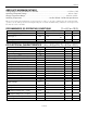
RECOMMENDED DC OPERATING CONDITIONS (T
A
= 0C to +70C)
PARAMETER SYMBOL MIN TYP MAX UNITS NOTES
Power Supply Voltage V
CC
4.5 5.0 5.5 V 1
Input Logic 1 V
IH
2.0
V
CC
+
0.3
V 1
Input Logic 0 V
IL
-0.3 +0.8 V 1
Battery Voltage V
BAT
2.5 3.7 V 1
DC ELECTRICAL CHARACTERISTICS (V
CC
= 5.0V ±10%, T
A
= 0C to +70C.)
PARAMETER SYMBOL MIN TYP MAX UNITS NOTES
Input Leakage I
LI
-1 +1
A
CS Leakage I
LO
150
A
7
Logic 1 Output (I
OUT
= -0.4mA) V
OH
2.4 V 1
Logic 0 Output (I
OUT
= 1.5mA) V
OL
0.4 V 1
Active Supply Current (CS = V
CC
- 0.2) I
CCA
1.5 2.0 mA 2
ADC Current I
ADC
500
A
3
Standby Current (CS = V
IL
) I
CCS
300
A
4
Battery Current (Oscillator On) I
BAT
300 500 nA
Battery Current (Oscillator Off) I
BAT
200 nA
Internal RST Pullup Resistor
R
P
35 47 60
k
V
CC
Trip Point V
CCTP
4.25 4.35 4.50 V
V
CC
Switchover V
CCSW
2.60 2.70 2.80 V 10
A/D Reference Voltage V
ADC
2.47 2.55 2.63 V
Pushbutton Detect PB
DV
0.8 2.0 V
Pushbutton Release PB
RD
0.3 0.8 V
Output Voltage V
CCO
V
CC
-
0.3
V 9
PFI Input Threshold V
PFI
1.20 1.25 1.30 V
PFI Input Current I
PFI
0.25 0.01 25 nA
PFO Output Voltage (I
OH
= -1A)
V
OH
V
CC
-
1.5
V
PFO Output voltage (I
OL
= 3.2A)
V
OL
0.4 V
V
CCO
Output Current (Source = V
CC
) I
CCO1
150 mA 11
V
CCO
Output Current (Source = V
BAT)
I
CCO2
150
A
12