
Datasheet
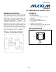


DS1672
7 of 15
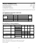
PIN DESCRIPTION
PIN NAME FUNCTION
1, 2 X1, X2
Connections for Standard 32.768kHz Quartz Crystal. The internal oscillator
circuitry is designed for operation with a crystal having a specified load
capacitance (CL) of 6pF. For more information about crystal selection and
crystal layout considerations, refer to Application Note 58: Crystal
Considerations with Dallas Real-Time Clocks. The DS1672 can also be driven
by an external 32.768kHz oscillator. In this configuration, the X1 pin is
connected to the external oscillator signal and the X2 pin is left unconnected
.
3 V
BACKUP
Battery Input for Any Standard 3V Lithium Cell or Other Energy Source.
Battery voltage must be held between 1.3V and 3.63V for proper operation.
Diodes placed in series between the power source and the V
BACKUP
pin may
result in improper operation. If a backup supply is not required, V
BACKUP
must
be grounded. UL recognized to ensure against reverse charging current when
used in conjunction with a lithium battery (charger disabled). See “Conditions
of Acceptability” at www.maxim-ic.com/qa/info/ul.
4 GND Ground.
5 SDA
Serial-Data Input/Output. SDA is the input/output pin for the I
2
C serial
interface. The SDA pin is open drain and requires an external pullup resistor.
6 SCL
I
2
C Serial-Clock Input. SCL is used to synchronize data movement on the
serial interface and requires an external pullup resistor.
7 RST
Active-Low Reset Output. It functions as a microprocessor reset signal. This
pin is an open-drain output and requires an external pullup resistor.
8 V
CC
Power pin for Primary Power Supply. When V
CC
is applied within normal
limits, the device is fully accessible and data can be written and read. When
V
CC
is below V
PF
, reads and writes are inhibited.
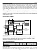
Figure 3. Recommended Layout for Crystal
LOCAL GROUND PLANE (LAYER 2)
CRYSTAL
X1
X2
GND