
Datasheet


DS1672
3 of 15
ABSOLUTE MAXIMUM RATINGS
Voltage Range on Any Pin Relative to Ground……………………………………………..-0.5V to +6.0V
Operating Temperature Range (noncondensing) ...…………………………………………-40°C to +85°C
Storage Temperature Range……………………………………………………………….-55°C to +125°C
Soldering Temperature (reflow)………………………………………….…………………. +260°C
Lead Temperature (soldering, 10s) ……………………………………………………………….. +260°C
This is a stress rating only and functional operation of the device at these or any other conditions beyond those indicated in the operation
sections of this specification is not implied. Exposure to absolute maximum rating conditions for extended periods of time can affect device
reliability.
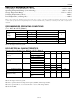
RECOMMENDED OPERATING CONDITIONS
(T
A
= -40°C to +85°C) (Note 1)
PARAMETER SYMBOL MIN TYP MAX UNITS
Supply
Voltage
DS1672-2
V
CC
1.8
2.0
5.5
V
DS1672-3
V
CC
2.7
3.0
5.5
DS1672-33
V
CC
2.97
3.3
5.5
Logic 1
V
IH
0.7 x V
CC
V
CC
+ 0.5
V
Logic 0
V
IL
-0.5
+0.3 x V
CC
V
Backup Supply Voltage
V
BACKUP
1.3
3.0
3.63
V
Note 1: All voltages referenced to ground.
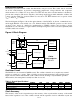
DC ELECTRICAL CHARACTERISTICS
(V
CCMIN
< V
CC
< V
CCMAX,
T
A
= -40°C to +85°C.) (Note 1)
PARAMETER
SYMBOL
CONDITIONS
MIN
TYP
MAX
UNITS
Active Supply Current
(Note 2)
I
CCA
-2: V
CC
= 2.2V
600
µA
-3: V
CC
= 3.3V
-33: V
CC
= 3.63V
Standby Current
(Note 3)
I
CCS
-2: V
CC
= 2.2V
500
µA
-3: V
CC
= 3.3V
-33: V
CC
= 3.63V
Power-Fail Voltage
V
PF
-2:
2.70
2.88
2.97
V
-3:
2.45
2.60
2.70
-33:
1.58
1.70
1.80
V
BACKUP
Leakage Current
I
BACKUPLKG
25
50
nA
Logic 0 Output (Note 4)
I
OL
V
OL
= 0.4V
3
mA
Logic 0 Output (Note 4,
DS1672-2 Only)
I
OL
V
CC
> 2V; V
OL
= 0.4V
3
mA
V
CC
< 2V; V
OL
= V
CC
* 0.2
Note 1: All voltages referenced to ground.
Note 2: I
CCA
specified with SCL clocking at max frequency (400kHz), trickle charger disabled.
Note 3: I
CCS
specified with V
CC
= V
CCTYP
and SDA, SCL = V
CCTYP
, trickle charger disabled.
Note 4: SDA and RST.