
Datasheet

SPI Serial-Data Bus
The DS1390/DS1391/DS1394 provide a 4-wire SPI seri-
al-data bus to communicate in systems with an SPI host
controller. The DS1390/DS1391 support SPI modes 1
and 3, while the DS1394 supports SPI modes 0 and 2.
Both devices support single-byte and multiple-byte data
transfers for maximum flexibility. The DIN and DOUT pins
are the serial-data input and output pins, respectively.
The CS input initiates and terminates a data transfer.
The SCLK pin synchronizes data movement between the
master (microcontroller) and the slave (DS1390/DS1391)
devices. The shift clock (SCLK), which is generated by
the microcontroller, is active only during address and data
transfer to any device on the SPI bus. Input data (DIN)
is latched on the internal strobe edge and output data
(DOUT) is shifted out on the shift edge (Figure 9). There
is one clock for each bit transferred. Address and data bits
are transferred in groups of eight.
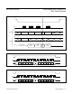
Address and data bytes are shifted MSB first into the
serial-data input (DIN) and out of the serial-data output
(DOUT). Any transfer requires the address of the byte to
specify a write or read, followed by one or more bytes of
data. Data is transferred out of the DOUT pin for a read
operation and into the DIN for a write operation (Figures
10 and 11).
The address byte is always the first byte entered after CS
is driven low. The most significant bit (W/R) of this byte
determines if a read or write takes place. If W/R is 0, one
or more read cycles occur. If W/R is 1, one or more write
cycles occur.
Data transfers can occur one byte at a time or in multi-
ple-byte burst mode. After CS is driven low, an address
is written to the DS1390/DS1391/DS1394. After the
address, one or more data bytes can be written or read.
For a single-byte transfer, one byte is read or written
and then CS is driven high. For a multiple-byte trans-
fer, however, multiple bytes can be read or written after
the address has been written. Each read or write cycle
causes the RTC register address to automatically incre-
ment. Incrementing continues until the device is disabled.
The address wraps to 00h after incrementing to 0Fh (dur-
ing a read) and wraps to 80h after incrementing to 8Fh
(during a write). Note, however, that an updated copy of
the time is only loaded into the user-accessible copy upon
the falling edge of CS. Reading the RTC registers in a
continuous loop does not show the time advancing.
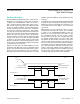
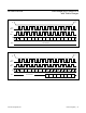
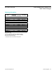
Figure 9. Serial Clock as a Function of Microcontroller Clock-Polarity Bit
CPHA = 0
CPHA = 1
CS
SHIFT DATA OUT (READ)
MODE 0
MODE 2
DATA LATCH/SAMPLE (WRITE)
SCLK WHEN CPOL = 0
SHIFT DATA OUT (READ)
DATA LATCH/SAMPLE (WRITE)
DATA LATCH/SAMPLE (WRITE)
MODE 1
MODE 3
SHIFT DATA OUT (READ)
DATA LATCH/SAMPLE (WRITE)
SHIFT DATA OUT (READ)
SCLK WHEN CPOL = 1
www.maximintegrated.com
Maxim Integrated
│
21
DS1390–DS1394 Low-Voltage SPI/3-Wire RTCs
with Trickle Charger