
Datasheet

The user determines diode and resistor selection accord-
ing to the maximum current desired for battery or super
cap charging. The maximum charging current can be
calculated as illustrated in the following example. Assume
that a system power supply of 3.3V is applied to V
CC
and
a super cap is connected to V
BACKUP
. Also, assume that
the trickle charger has been enabled with a diode and
resistor R2 between V
CC
and V
BACKUP
. The maximum
current I
MAX
would therefore be calculated as follows:
I
MAX
= (3.3V - diode drop) / R2 ≈ (3.3V - 0.7V) /
2kΩ ≈ 1.3mA
As the super cap changes, the voltage drop between V
CC
and V
BACKUP
decreases and therefore the charge cur-
rent decreases.
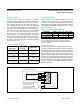
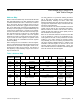
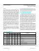
Table 6. SPI Pin Function
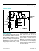
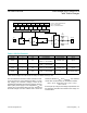
Figure 8. DS1390–DS1394 Programmable Trickle Charger
*CPOL is the clock-polarity bit set in the control register of the host microprocessor.
**SDO remains at high-Z until 8 bits of data are ready to be shifted out during a read.
MODE CPHA CS SCLK SDI SDO
Disable X High Input Disabled Input Disabled High-Z
Write 0 Low
CPOL* = 0, SCLK Rising;
CPOL = 1, SCLK Falling
Data Bit Latch High-Z
Read 0 Low
CPOL = 0, SCLK Falling;
CPOL = 1, SCLK Rising
X Next Data Bit Shift**
Write 1 Low
CPOL* = 1, SCLK Rising;
CPOL = 0, SCLK Falling
Data Bit Latch High-Z
Read 1 Low
CPOL = 1, SCLK Falling;
CPOL = 0, SCLK Rising
X Next Data Bit Shift**
R1
250W
R2
2kW
R3
4kW
V
CC
V
BACKUP
BIT 7
BIT 6 BIT 5 BIT 4 BIT 3 BIT 2 BIT 1 BIT 0
TCS3 TCS2 TCS1 TCS0 DS1 DS0 ROUT1 ROUT0
TRICKLE-CHARGE REGISTER (8Fh WRITE, 0Fh READ)
1 0F 16 SELECT
NOTE: ONLY 1010b ENABLES CHARGER
1 OF 2
SELECT
1 OF 3
SELECT
TCS[3:0] = TRICKLE-CHARGE SELECT
DS[1:0] = DIODE SELECT
ROUT[1:0] = RESISTOR SELECT
www.maximintegrated.com
Maxim Integrated
│
20
DS1390–DS1394 Low-Voltage SPI/3-Wire RTCs
with Trickle Charger