
Datasheet

Special-Purpose Registers
The DS1390–DS1394 have three additional registers
(control, status, and trickle charger) that control the RTC,
alarms, square-wave output, and trickle charger.
Bit 7: Enable Oscillator (EOSC). When set to logic 0,
this bit starts the oscillator. When this bit is set to logic 1,
the oscillator is stopped whenever the device is powered
by V
BACKUP
. The oscillator is always enabled when V
CC
is valid. This bit is enabled (logic 0) when V
CC
is first
applied.
Bit 5: Battery-Backed Square-Wave and Interrupt
Enable (BBSQI). This bit when set to logic 1 enables the
square wave or interrupt output when V
CC
is absent and
the DS1390/DS1392/DS1393/DS1394 are being pow-
ered by the V
BACKUP
pin. When BBSQI is logic 0, the
SQW/INT pin (or SQW and INT pins) goes high imped-
ance when V
CC
falls below the power-fail trip point. This
bit is disabled (logic 0) when power is first applied.
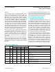
Bits 4 and 3: Rate Select (RS2 and RS1). These bits
control the frequency of the square-wave output when the
square wave has been enabled. The table below shows
the square-wave frequencies that can be selected with
the RS bits. These bits are both set to logic 1 (32kHz)
when power is first applied.
Bit 2: Interrupt Control (INTCN). This bit controls the
SQW/INT signal. When the INTCN bit is set to logic 0, a
square wave is output on the SQW/INT pin. The oscillator
must also be enabled for the square wave to be out-put.
When the INTCN bit is set to logic 1, a match between
the timekeeping registers and either of the alarm registers
then activates the SQW/INT (provided the alarm is also
enabled). The corresponding alarm flag is always set,
regardless of the state of the INTCN bit. The INTCN bit is
set to logic 0 when power is first applied.
Bit 0: Alarm Interrupt Enable (AIE). When set to logic 1,
this bit permits the alarm flag (AF) bit in the status register
to assert SQW/INT (when INTCN = 1). When the AIE bit is
set to logic 0 or INTCN is set to logic 0, the AF bit does not
initiate the SQW/INT signal. The AIE bit is disabled (logic
0) when power is first applied.
Control bits used in the DS1390 become general-pur-
pose, battery-backed, nonvolatile SRAM bits in the
DS1391.
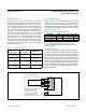
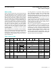
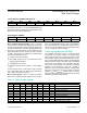
BIT 7 BIT 6 BIT 5 BIT 4 BIT 3 BIT 2 BIT 1 BIT 0
EOSC 0 BBSQI RS2 RS1 INTCN 0 AIE
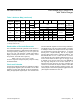
BIT 7 BIT 6 BIT 5 BIT 4 BIT 3 BIT 2 BIT 1 BIT 0
EOSC 0 X X X X 0 X
RS2 RS1 SQUARE-WAVE OUTPUT FREQUENCY
0 0 1Hz
0 1 4.096kHz
1 0 8.192kHz
1 1 32.768kHz
www.maximintegrated.com
Maxim Integrated
│
18
DS1390–DS1394 Low-Voltage SPI/3-Wire RTCs
with Trickle Charger
Control Register (0D/8Dh) (DS1390/DS1393/DS1394 Only)
Control Register (0D/8Dh) (DS1391 Only)