
Datasheet

Alarms
All five devices contain one time-of-day/date alarm.
Writing to registers 88h through 8Ch sets the alarm. The
alarm can be programmed (by the alarm enable and
INTCN bits of the control register) to activate the SQW/
INT or INT output on an alarm-match condition. The alarm
can activate the SQW/INT or INT output while the device
is running from V
BACKUP
if BBSQI is enabled. Bit 7 of
each of the time-of-day/date alarm registers are mask bits
(Table 4). When all the mask bits for each alarm are logic
0, an alarm only occurs when the values in the timekeep-
ing registers 00h to 06h match the values stored in the
time-of-day/date alarm registers. The alarms can also be
programmed to repeat every second, minute, hour, day, or
date. Table 4 shows the possible settings. Configurations
not listed in the table result in illogical operation.
The DY/DT bits (bit 6 of the alarm day/date registers)
control whether the alarm value stored in bits 0 to 5 of
that register reflects the day of the week or the date of
the month. If DY/DT is written to logic 0, the alarm is the
result of a match with date of the month. If DY/DT is writ-
ten to a logic 1, the alarm is the result of a match with day
of the week.
When the RTC register values match alarm register set-
tings, the alarm-flag (AF) bit is set to logic 1. If the alarm-
interrupt enable (AIE) is also set to logic 1 and the INTCN
bit is set to logic 1, the alarm condition activates the SQW/
INT signal.
Since the contents of register 08h are expected to nor-
mally contain a match value of 00–99 decimal, the codes
F[0–9], and FF have been used to tell the part to mask the
tenths or hundredths of seconds accordingly.
Power-Up/Down, Reset, and
Pushbutton Reset Functions
A precision temperature-compensated reference and
comparator circuit monitors the status of V
CC
. When an
out-of-tolerance condition occurs, an internal power-fail
signal is generated that blocks read/write access to the
device and forces the RST pin (DS1391/DS1393 only)
low. When V
CC
returns to an in-tolerance condition, the
internal power-fail signal is held active for t
RST
to allow
the power supply to stabilize, and the RST (DS1391/
DS1393 only) pin is held low. If the EOSC bit is set to logic
1 (to disable the oscillator in battery-backup mode), the
internal power-fail signal and the RST pin is kept active
for t
RST
plus the startup time of the oscillator.
The DS1391/DS1393 provide for a pushbutton switch to
be connected to the RST output pin. When the DS1391/
DS1393 are not in a reset cycle, it continuously moni-
tors the RST signal for a low-going edge. If an edge is
detected, the part debounces the switch by pulling the
RST pin low and inhibits read/write access. After PB
DB
has expired, the part continues to monitor the RST line. If
the line is still low, it continues to monitor the line looking
for a rising edge. Upon detecting release, the part forces
the RST pin low and holds it low for an additional PB
DB.
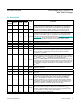
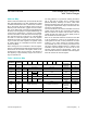
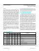
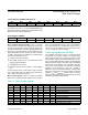
Table 4. Alarm Mask Bits
REGISTER
08H
DY/DT
ALARM REGISTER MASK BITS (BIT 7)
ALARM RATE
AM4 AM3 AM2 AM1
FFh X 1 1 1 1 Alarm every 1/100th of a second
F[0–9]h X 1 1 1 1 Alarm when hundredths of seconds match
[0–9][0–9] X 1 1 1 1 Alarm when tenths, hundredths of seconds match
[0–9][0–9] X 1 1 1 0
Alarm when seconds, tenths, and hundredths of seconds
match
[0–9][0–9] X 1 1 0 0
Alarm when minutes, seconds, tenths, and hundredths of
seconds match
[0–9][0–9] X 1 0 0 0
Alarm when hours, minutes, seconds, tenths, and hundredths
of seconds match
[0–9][0–9] 0 0 0 0 0
Alarm when date, hours, minutes, seconds, tenths, and
hundredths of seconds match
[0–9][0–9] 1 0 0 0 0
Alarm when day, hours, minutes, seconds, tenths, and
hundredths of seconds match
www.maximintegrated.com
Maxim Integrated
│
17
DS1390–DS1394 Low-Voltage SPI/3-Wire RTCs
with Trickle Charger