
Datasheet

Address Map
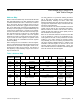
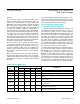
Table 3 shows the address map for the DS1390–DS1393
RTC and RAM registers. The RTC registers are located
in address locations 00h to 0Fh in read mode, and 80h to
8Fh in write mode. During a multibyte access, when the
address pointer reaches 0Fh, it wraps around to location
00h. On the falling edge of the CS pin (DS1390/DS1391/
DS1394) or the rising edge of CE (DS1392/DS1393), the
current time is transferred to a second set of registers.
The time information is read from these secondary regis-
ters, while the clock may continue to run. This eliminates
the need to re-read the registers if the main registers
update during a read. To avoid rollover issues when writ-
ing to the time and date registers, all registers should
be written before the hundredths-of-seconds registers
reaches 99 (BCD).
When reading from the hundredths of seconds register,
there is a possibility that the data transfer happens at the
same time as an increment of the register. If this occurs,
the data in the buffer may be incorrect. The chances of
this happening is approximately 170ppb. There are two
ways to deal with this.
The first method is to synchronize enabling the device
(CE or CS) with the square wave or interrupt output
(DS1390–DS1394). Enabling the device, either after
detecting the falling edge of the interrupt output or the ris-
ing edge of the square-wave output, ensures that the two
events are not simultaneous.
The second method is to read the hundredths of seconds
register until the data for two consecutive reads match.
With this method, the master must be able to read the
register at least twice within the 10ms update period of
the hundredths of seconds register.
Either of the described methods ensures that the data
in all the registers is correct. If the hundredths of sec-
onds register is not used, it is also possible for the same
problem to occur when reading the seconds register.
The probability of an error is inversely proportional to the
rate of the register's update frequency in relation to the
hundredth of seconds register, so the error rate for the
seconds register would be approximately 1.7ppb. The
same methods used for the hundredth of seconds register
would be used for the seconds register.
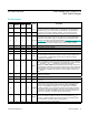
Table 3. Address Map
WRITE
ADDRE
SS
READ
ADDRESS
BIT 7 BIT 6 BIT 5 BIT 4 BIT 3 BIT 2 BIT 1 BIT 0 FUNCTION RANGE
80h 00h Tenths of Seconds Hundredths of Seconds
Hundredths of
Seconds
0–99 BCD
81h 01h 0 10 Seconds Seconds Seconds 00–59 BCD
82h 02h 0 10 Minutes Minutes Minutes 00–59 BCD
83h 03h 0 12/24
AM/PM
10
Hour
Hour Hours
1–12 +AM/PM
00–23 BCD
10 Hour
84h 04h 0 0 0 0 0 Day Day 1–7 BCD
85h 05h 0 0 10 Date Date Date 01–31 BCD
86h 06h Century 0 0
10
Month
Month
Month/
Century
01–12 +
Century BCD
87h 07h 10 Year Year Year 00–99 BCD
88h 08h Tenths of Seconds Hundredths of Seconds
Alarm
Hundredths of
Seconds
0–99 BCD
89h 09h AM1 10 Seconds Seconds
Alarm
Seconds
00–59 BCD
8Ah 0Ah AM2 10 Minutes Minutes Alarm Minutes 00–59 BCD
www.maximintegrated.com
Maxim Integrated
│
15
DS1390–DS1394 Low-Voltage SPI/3-Wire RTCs
with Trickle Charger