
Datasheet

Power Control
The power-control function is provided by a precise,
temperature-compensated voltage reference and a com-
parator circuit that monitors the V
CC
level. The device is
fully accessible and data can be written and read when
V
CC
is greater than V
PF
. However, when V
CC
falls below
V
PF
, the internal clock registers are blocked from any
access. If V
PF
is less than V
BACKUP
, the device power is
switched from V
CC
to V
BACKUP
when V
CC
drops below
V
PF
. If V
PF
is greater than V
BACKUP
, the device power
is switched from V
CC
to V
BACKUP
when V
CC
drops
below V
BACKUP
. Timekeeping operation and register
data are maintained from the V
BACKUP
source until V
CC
is returned to nominal levels (Table 1). After V
CC
returns
above V
PF
, read and write access is allowed after RST
goes high (Figure 5).
Oscillator Circuit
All five devices use an external 32.768kHz crystal. The
oscillator circuit does not require any external resistors
or capacitors to operate. Table 2 specifies several crystal
parameters for the external crystal. If a crystal is used with
the specified characteristics, the startup time is usually
less than one second.
Clock Accuracy
The accuracy of the clock is dependent upon the accu-
racy of the crystal and the accuracy of the match between
the capacitive load of the oscillator circuit and the capaci-
tive load for which the crystal was trimmed. Additional
error is added by crystal frequency drift caused by tem-
perature shifts. External circuit noise coupled into the
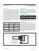
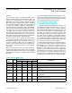
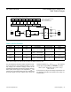
oscillator circuit can result in the clock running fast. Figure
7 shows a typical PC board layout for isolation of the crys-
tal and oscillator from noise. Refer to Application Note 58:
Crystal Considerations with Maxim Real-Time Clocks for
detailed information.
*The crystal, traces, and crystal input pins should be isolated
from RF generating signals. Refer to Application Note 58:
Crystal Considerations for Maxim Real-Time Clocks for addi-
tional specifications.
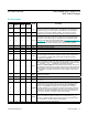
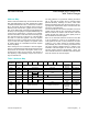
Table 1. Power Control
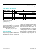
Table 2. Crystal Specifications*
Figure 7. Layout Example
SUPPLY
CONDITION
READ/WRITE
ACCESS)
POWERED BY
V
CC
< V
PF
,
V
CC
< V
BACKUP
No V
BACKUP
V
CC
< V
PF
,
V
CC
> V
BACKUP
No V
CC
V
CC
> V
PF
,
V
CC
< V
BACKUP
Yes V
CC
V
CC
> V
PF
,
V
CC
> V
BACKUP
Yes V
CC
PARAMETER SYMBOL MIN TYP MAX UNITS
Nominal Frequency f
O
32.768 kHz
Series Resistance ESR 55 kΩ
Load Capacitance C
L
6 pF
LOCAL GROUND PLANE (LAYER 2)
CRYSTAL
GND
X2
X1
NOTE: AVOID ROUTING SIGNAL LINES
IN THE CROSSHATCHED AREA
(UPPER LEFT QUADRANT) OF
THE PACKAGE UNLESS THERE IS
A GROUND PLANE BETWEEN THE
SIGNAL LINE AND THE DEVICE PACKAGE.
www.maximintegrated.com
Maxim Integrated
│
14
DS1390–DS1394 Low-Voltage SPI/3-Wire RTCs
with Trickle Charger