
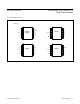
Datasheet
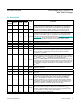
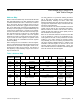
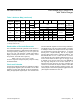
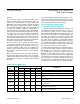

PIN
NAME
FUNCTION
DS1390/
DS1394
DS1391 DS1392 DS1393
1 1 1 1
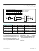
X1
Connections for Standard 32.768kHz Quartz Crystal. The internal oscillator
circuitry is designed for operation with a crystal having a 6pF specied load
capacitance (C
L
). Pin X1 is the input to the oscillator and can optionally be
connected to an external 32.768kHz oscillator. The output of the internal
oscillator, pin X2, is oated if an external oscillator is connected to pin X1.
2 2 2 2 X2
3 3 3 3 V
BACKUP
DC Backup Power Input for Primary Cell. This pin is a rechargeable battery/
super cap or a secondary supply. UL recognized to ensure against reverse
charging current when used with a lithium battery (http://www.maximintegrated.
com/qa/info/w/). This pin must be grounded if not used. Diodes in series
between the battery and the V
BACKUP
pin may prevent proper operation.
4 4 — — CS SPI Chip-Select Input. This pin is used to select or deselect the part.
— — 4 4 CE Chip Enable for 3-Wire Interface
5 5 5 5 GND Ground
6 6 — — DIN SPI Data Input. This pin is used to shift address and data into the part.
— — 6 — INT
Interrupt Output. This pin is used to output the interrupt signal, if enabled by
the control register. The maximum voltage on this pin is 5.5V, independent of
V
CC
or V
BACKUP
. If enabled, INT functions when the device is powered
by either V
CC
or V
BACKUP
.
— 9 — 6 RST
Reset. This active-low, open-drain output indicates the status of V
CC
relative to
the V
PF
specication. As V
CC
falls below V
PF
, the RST pin is driven low. When
V
CC
exceeds V
PF
, for t
RST
, the RST pin is driven high impedance.
This pin is combined with a debounced pushbutton input function. This pin can
be activated by a pushbutton reset request. This pin has an internal, 50kΩ (typ)
pullup resistor to V
CC
. No external pullup resistors should be connected. If the
crystal oscillator is disabled, the startup time of the oscillator is added to the
t
RST
delay.
7 7 — — DOUT
SPI Data Output. Data is output on this pin when the part is in read mode.
CMOS push-pull driver.
— — 7 7 I/O Input/Output for 3-Wire Interface. CMOS push-pull driver.
8 8 8 8 SCLK
Serial Clock Input. This pin is used to control the timing of data into and out
of the part.
9 — — 9 SQW/INT
Square-Wave/Interrupt Output. This pin is used to output the programmable
square wave or interrupt signal. When enabled by setting the ESQW bit
to logic 1, the SQW/INT pin outputs one of four frequencies: 32.768kHz,
8.192kHz, 4.096kHz, or 1Hz. This pin is open drain and requires an external
pullup resistor. The maximum voltage on this pin is 5.5V, independent of V
CC
or V
BACKUP
. If enabled, SQW/INT functions when the device is powered by
either V
CC
or V
BACKUP
. If not used, this pin can be left open.
— — 9 — SQW
Square-Wave Output. This pin is open drain and requires an external pullup
resistor. The maximum voltage on this pin is 5.5V, independent of V
CC
or
V
BACKUP
. If enabled, SQW functions when the device is powered by either
V
CC
or V
BACKUP
. If not used, this pin can be left open.
10 10 10 10 V
CC
DC Power Pin for Primary Power Supply
www.maximintegrated.com
Maxim Integrated
│
12
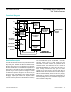
DS1390–DS1394 Low-Voltage SPI/3-Wire RTCs
with Trickle Charger
Pin Description