
Datasheet


DS1390–DS1394
Low-Voltage SPI/3-Wire RTCs with
Trickle Charger
19
Maxim Integrated
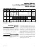
The user determines diode and resistor selection
according to the maximum current desired for battery
or super cap charging. The maximum charging current
can be calculated as illustrated in the following exam-
ple. Assume that a system power supply of 3.3V is
applied to V
CC
and a super cap is connected to
V
BACKUP
. Also, assume that the trickle charger has
been enabled with a diode and resistor R2 between
V
CC
and V
BACKUP
. The maximum current I
MAX
would
therefore be calculated as follows:
I
MAX
= (3.3V - diode drop) / R2 ≈ (3.3V - 0.7V) /
2kΩ≈1.3mA
As the super cap changes, the voltage drop between
V
CC
and V
BACKUP
decreases and therefore the charge
current decreases.
R1
250Ω
R2
2kΩ
R3
4kΩ
V
CC
V
BACKUP
BIT 7
BIT 6 BIT 5 BIT 4 BIT 3 BIT 2 BIT 1 BIT 0
TCS3 TCS2 TCS1 TCS0 DS1 DS0 ROUT1 ROUT0
TRICKLE-CHARGE REGISTER (8Fh WRITE, 0Fh READ)
1 0F 16 SELECT
NOTE: ONLY 1010b ENABLES CHARGER
1 OF 2
SELECT
1 OF 3
SELECT
TCS[3:0] = TRICKLE-CHARGE SELECT
DS[1:0] = DIODE SELECT
ROUT[1:0] = RESISTOR SELECT
Figure 8. DS1390–DS1394 Programmable Trickle Charger
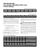
MODE CPHA CS SCLK SDI SDO
Disable X High Input Disabled Input Disabled High-Z
Write 0 Low
CPOL* = 0, SCLK Rising;
CPOL = 1, SCLK Falling
Data Bit Latch High-Z
Read 0 Low
CPOL = 0, SCLK Falling;
CPOL = 1, SCLK Rising
X Next Data Bit Shift**
Write 1 Low
CPOL* = 1, SCLK Rising;
CPOL = 0, SCLK Falling
Data Bit Latch High-Z
Read 1 Low
CPOL = 1, SCLK Falling;
CPOL = 0, SCLK Rising
X Next Data Bit Shift**
Table 6. SPI Pin Function
*
CPOL is the clock-polarity bit set in the control register of the host microprocessor.
**
SDO remains at high-Z until 8 bits of data are ready to be shifted out during a read.