
Datasheet


DS1374
Power Control
The power-control function is provided by a precise,
temperature-compensated voltage reference and a
comparator circuit that monitors the V
CC
level. The
device is fully accessible and data can be written and
read when V
CC
is greater than V
PF
. However, when
V
CC
falls below V
PF
, the internal clock registers are
blocked from any access. If V
PF
is less than V
BACKUP
,
the device power is switched from V
CC
to V
BACKUP
when V
CC
drops below V
PF
. If V
PF
is greater than
V
BACKUP
, the device power is switched from V
CC
to
V
BACKUP
when V
CC
drops below V
BACKUP
. The regis-
ters are maintained from the V
BACKUP
source until V
CC
is returned to nominal levels (Table 1). After V
CC
returns above V
PF
, read and write access is allowed
after RST goes high (Figure 1).
Address Map
Table 3 shows the address map for the DS1374 regis-
ters. During a multibyte access, the address pointer
wraps around to location 00h when it reaches the end of
the register space (08h). On an I
2
C START, STOP, or
address pointer incrementing to location 00h, the current
time is transferred to a second set of registers. These
secondary registers read the time information, while the
clock continues to run. This eliminates the need to reread
the registers in case of an update of the main registers
during a read.
Time-of-Day Counter
The time-of-day counter is a 32-bit up counter that
increments once per second when the oscillator is run-
ning. The contents can be read or written by accessing
the address range 00h–03h. When the counter is read,
the current time of day is latched into a register, which
is output on the serial data line while the counter contin-
ues to increment.
Note: Writing to any TOD register will reset the 1Hz
square wave output.
I
2
C, 32-Bit Binary Counter Watchdog RTC with
Trickle Charger and Reset Input/Output
10 ____________________________________________________________________
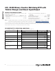
SUPPLY CONDITION
READ/WRITE
ACCESS
POWERED
BY
V
CC
< V
PF
, V
CC
< V
BACKPUP
No V
BACKUP
V
CC
< V
PF
, V
CC
> V
BACKUP
No V
CC
V
CC
> V
PF
, V
CC
< V
BACKUP
Yes V
CC
V
CC
> V
PF
, V
CC
> V
BACKUP
Yes V
CC
Table 2. Power Control
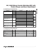
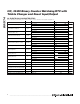
ADDRESS BIT 7 BIT 6 BIT 5 BIT 4 BIT 3 BIT 2 BIT 1 BIT 0 FUNCTION
00H TOD Counter Byte 0 Time-of-Day Counter
01H TOD Counter Byte 1 Time-of-Day Counter
02H TOD Counter Byte 2 Time-of-Day Counter
03H TOD Counter Byte 3 Time-of-Day Counter
04H WD/ALM Counter Byte 0 Watchdog/Alarm Counter
05H WD/ALM Counter Byte 1 Watchdog/Alarm Counter
06H WD/ALM Counter Byte 2 Watchdog/Alarm Counter
07H EOSC WACE WD/ALM BBSQW WDSTR RS2 RS1 AIE Control
08H OSF 0 0 0 0 0 0 AF Status
09H TCS3 TCS2 TCS1 TCS0 DS1 DS0 ROUT1 ROUT0 Trickle Charger
Table 3. Address Map
Note: Unless otherwise specified, the state of the registers is not defined when power is first applied.