
Datasheet


Low-Current, SPI-Compatible
Real-Time Clock
8 Maxim Integrated
DS1347
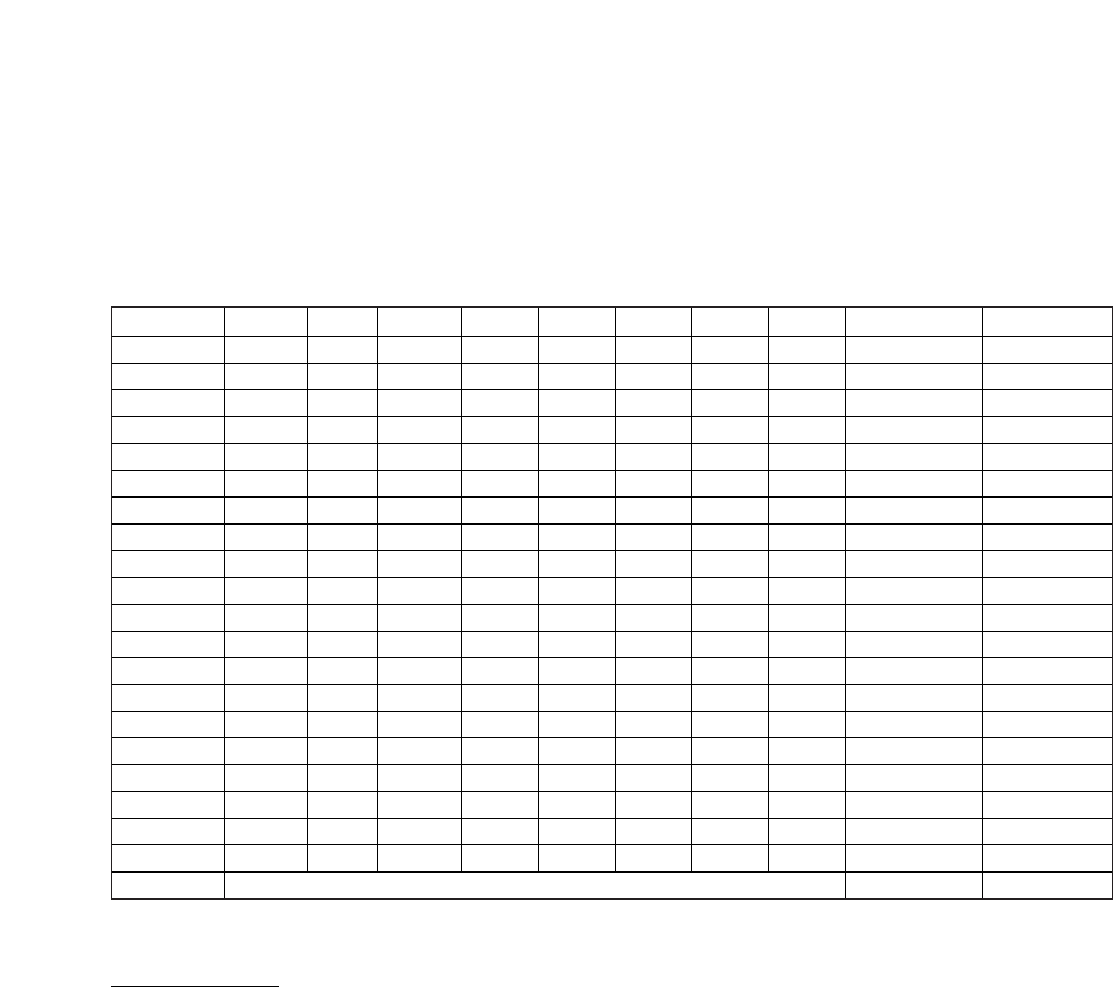
ADDRESS BIT 7 BIT 6 BIT 5 BIT 4 BIT 3 BIT 2 BIT 1 BIT 0 FUNCTION RANGE
57h X X X X X X X X RAM 11 00h–FFh
59h X X X X X X X X RAM 12 00h–FFh
5Bh X X X X X X X X RAM 13 00h–FFh
5Dh X X X X X X X X RAM 14 00h–FFh
5Fh X X X X X X X X RAM 15 00h–FFh
61h X X X X X X X X RAM 16 00h–FFh
63h X X X X X X X X RAM 17 00h–FFh
65h X X X X X X X X RAM 18 00h–FFh
67h X X X X X X X X RAM 19 00h–FFh
69h X X X X X X X X RAM 20 00h–FFh
6Bh X X X X X X X X RAM 21 00h–FFh
6Dh X X X X X X X X RAM 22 00h–FFh
6Fh X X X X X X X X RAM 23 00h–FFh
71h X X X X X X X X RAM 24 00h–FFh
73h X X X X X X X X RAM 25 00h–FFh
75h X X X X X X X X RAM 26 00h–FFh
77h X X X X X X X X RAM 27 00h–FFh
79h X X X X X X X X RAM 28 00h–FFh
7Bh X X X X X X X X RAM 29 00h–FFh
7Dh X X X X X X X X RAM 30 00h–FFh
7Fh See the Data Input (Burst Write) section. RAM Burst —
Table 1. Register Map (continued)
Command and Control
Address/Command Byte
Each data transfer into or out of the device is initiated by
an address/command byte. The address/command byte
specifies which registers are to be accessed, and if the
access is a read or a write. Table 1 shows the
address/command bytes and their associated regis-
ters, and lists the hex codes for all read and write oper-
ations. The address/command bytes are input MSB
(bit 7) first. Bit 7 specifies a write (logic 0) or read
(logic 1). Bit 6 specifies register data (logic 0) or RAM
data (logic 1). Bits 5–1 specify the designated register
to be written or read. The LSB (bit 0) must be logic 1. If
the LSB is a zero, writes to the device are disabled.
Clock Burst Mode
Sending the clock burst address/command (3Fh) spec-
ifies burst-mode operation. In this mode, multiple bytes
are read or written after a single address/command.
The first seven clock/calendar registers (Seconds,
Minutes, Hours, Date, Month, Day, and Year) and the
Control register are consecutively read or written, start-
ing with the MSB of the Seconds register. When writing
to the clock registers in burst mode, all seven clock/cal-
endar registers and the Control register must be written
in order for the data to be transferred. See the
Example:
Setting the Clock with a Burst Write
section.
RAM Burst Mode
Sending the RAM burst address/command (7Fh) speci-
fies burst-mode operation. In this mode, the 31 RAM
locations can be consecutively read or written, starting
at 41h. When writing to RAM in burst mode, it is not
necessary to write all 31 bytes for the data to transfer;
each complete byte written is transferred to RAM. When
reading from RAM, data is output until all 31 bytes have
been read, or until CS is driven high.
0 = Reads as logic 0, 1 = Reads as logic 1, X = Don’t care.