
Datasheet


Low-Current, SPI-Compatible
Real-Time Clock
Maxim Integrated 5
DS1347
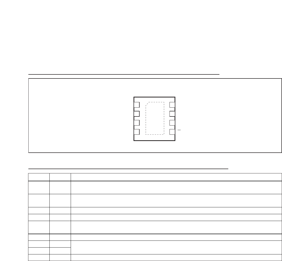
Pin Configuration
V
CC
CSGND
1
2
8
7
X1
X2DOUT
DIN
SCLK
TDFN
TOP VIEW
3
4
6
5
DS1347
+
EP
Pin Description
PIN NAME FUNCTION
1 SCLK
Serial-Clock Input. SCLK is used to synchronize data movement on the serial interface for either 3-wire or
SPI communications.
2 DOUT
Serial-Data Output. When SPI communication is enabled, the DOUT pin is the serial-data output for the SPI
bus.
3 DIN Serial-Data Input. When SPI communication is enabled, the DIN pin is the serial-data input for the SPI bus.
4 GND Ground
5 CS
Active-Low Chip Select. The chip-enable signal must be asserted low during a read or a write for SPI
communications.
6 V
CC
Power-Supply Input
7 X2
8 X1
Connections for Standard 32.768kHz Quartz Crystal (see the Crystal Characteristics table).
— EP Exposed Pad. Connect to GND or leave unconnected.