
Datasheet


Low-Current, SPI-Compatible
Real-Time Clock
Maxim Integrated 3
DS1347
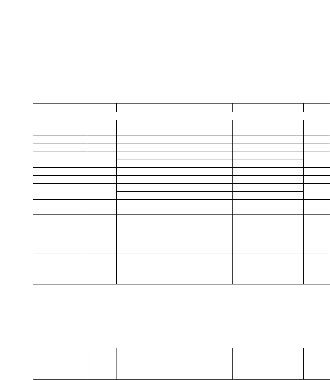
AC ELECTRICAL CHARACTERISTICS
(V
CC
= +2.0V to +5.5V, T
A
= -40°C to +85°C. Typical values are at V
CC
= +3.3V, T
A
= +25°C, unless otherwise noted.)
(Figure 5, Notes 1, 5)
PARAMETER SYMBOL CONDITIONS MIN TYP MAX UNITS
SPI SERIAL TIMING
Input Rise Time t
rIN
DIN, SCLK, CS 5 ns
Input Fall Time t
fIN
DIN, SCLK, CS 5 ns
Output Rise Time t
rOUT
DOUT, C
LOAD
= 100pF 10 ns
Output Fall Time t
fOUT
DOUT, C
LOAD
= 100pF 10 ns
V
CC
= +2V 1000
SCLK Period t
CP
V
CC
= +5V 238
ns
SCLK High Time t
CH
100 ns
SCLK Low Time t
CL
100 ns
V
CC
= +2V, C
LOAD
= 100pF 300
SCLK Fall to DOUT
Valid
t
DO
V
CC
= +5V, C
LOAD
= 100pF 100
ns
DIN to SCLK Setup
Time
t
DS
100 ns
DIN to SCLK Hold
Time
t
DH
20 ns
V
CC
= +2V 200
SCLK Rise to CS
Rise Hold Time
t
CSH
V
CC
= +5V 50
ns
CS High Pulse Width t
CSW
200 ns
CS High to DOUT
High Impedance
t
CSZ
100 ns
CS to SCLK Setup
Time
t
CSS
100 ns
CRYSTAL CHARACTERISTICS
Note 1: All parameters are 100% tested at T
A
= +25°C. Limits over temperature are guaranteed by design and characterization and
not production tested.
Note 2: I
CC
is specified with DOUT open, CS = DIN = GND, SCLK = 4MHz at V
CC
= +5V; SCLK = 1MHz at V
CC
= +2.0V.
Note 3: Timekeeping current is specified with CS = V
CC
, SCLK = DIN = GND, DOSF = 0, EGFIL = 1.
Note 4: Guaranteed by design and not 100% production tested.
Note 5: All values referred to V
IH(MIN)
and V
IL(MAX)
levels.
PARAMETER SYMBOL CONDITIONS MIN TYP MAX UNITS
Nominal Frequency f
O
32.768 kHz
Series Resistance ESR 100 k
Load Capacitance C
L
12.5 pF