
Datasheet


9Maxim Integrated
Low-Current SPI/3-Wire RTCs
DS1343/DS1344
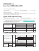
Pin Descriptions (continued)
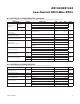
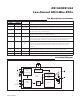
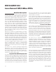
Functional Diagram
DS1343
DS1344
N
CLOCK, CALENDAR, AND
ALARM REGISTERS
OSCILLATOR AND
COUNTDOWN CHAIN
INT0
INPUT
SHIFT
REGISTER
CONTROL
REGISTERS
USER RAM
SERIAL
INTERFACE
N
INT1
SERMODE
SDO
SDI
SCLK
CE
POWER CONTROL
AND
TRICKLE CHARGER
GND
ON_VCC
1Hz
X2
32.768kHz
X1
V
BAT
PF
V
CC
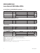
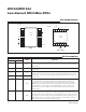
PIN
NAME FUNCTION
TSSOP TDFN-EP
10 7 GND Ground
11 13 SERMODE
Serial-Interface Mode Input. When connected to GND, standard 3-wire
communication is selected. When connected to V
CC
, SPI communication is selected.
12 8 CE
Chip Enable. The chip-enable signal must be asserted high during a read or a write
for either 3-wire or SPI communications.
14 9 SCLK
Serial-Clock Input. SCLK is used to synchronize data movement on the serial
interface for either 3-wire or SPI communications.
15 10 SDI
Serial-Data Input. When SPI communication is selected, SDI is the serial-data input
for the SPI bus. When 3-wire communication is selected, this pin must be connected
to SDO (SDI and SDO function as a single I/O pin when connected together).
16 11 SDO
Serial-Data Output. When SPI communication is selected, SDO is the serial-data
output for the SPI bus. When 3-wire communication is selected, this pin must be
connected to SDI (SDI and SDO function as a single I/O pin when connected
together).
18 12
PF
Active-Low Power-Fail Output. The PF pin is used to indicate loss of the primary
power supply (V
CC
). When V
CC
is less than V
PF
, the PF pin is driven low.
20 14 V
CC
Power-Supply Input
— — EP Exposed Pad (TDFN Only). Connect to GND or leave unconnected.