
Datasheet


6 Maxim Integrated
Low-Current I2C RTCs for High-ESR Crystals
DS1341/DS1342
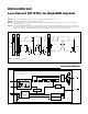
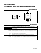
Pin Description
Pin Configurations
µSOP
2 7 SQW/INTBX2
1 8 V
CC
X1
SCLCLKIN/INTA 3 6
SDA
EP
GND 4 5
DS1341
DS1342
DS1341
DS1342
TOP VIEW
+
1 3 4
8 6 5
V
CC
SCL
SDA
2
7
SQW/
INTB
X1
X2
CLKIN/
INTA
GND
TDFN
+
PIN NAME FUNCTION
1 X1
Connections for a Standard 32.768kHz Quartz Crystal. The internal oscillator circuitry is
designed for operation with a crystal having a specified load capacitance (C
L
) of 6pF (DS1341)
or 12.5pF (DS1342).
2 X2
3
CLKIN/INTA
Clock Input/Active-Low Interrupt Output. This I/O pin is used to output an alarm interrupt or
accept an external clock input to drive the RTC counter. In the output mode, this is an open
drain and requires an external pullup resistor. If not used, connect this pin to ground.
4 GND Ground
5 SDA
Serial-Data Input/Output. SDA is the input/output pin for the I
2
C serial interface. The SDA pin is
open drain and requires an external pullup resistor.
6 SCL Serial-Clock Input. SCL is used to synchronize data movement on the serial interface.
7
SQW/INTB
Square-Wave/Active-Low Interrupt Output. This pin is used to output a programmable square
wave or an alarm interrupt signal. This is a CMOS push-pull output and does not require an
external pullup resistor. If not used, this pin can be left unconnected.
8 V
CC
DC Power Input. This pin should be decoupled using a 0.01FF or 0.1FF capacitor.
— EP Exposed Pad (TDFN Only). Connect to GND or leave unconnected.