
Datasheet


4 Maxim Integrated
Low-Current I2C RTCs for High-ESR Crystals
DS1341/DS1342
Note 11: C
B
is the total capacitance of one bus line, including all connected devices, in pF.
Note 12:
Guaranteed by design; not 100% production tested.
Note 13: The parameter t
OSF
is the period of time the oscillator must be stopped for the OSF flag to be set over the voltage
range of 2.4V P V
CC
P V
CCMAX
.
Note 14: The DS1341/DS1342 can detect any single SCL clock held low longer than t
TIMEOUTMIN
. The devices’ I
2
C interface is
in reset state and can receive a new START condition when SCL is held low for at least t
TIMEOUTMAX
. Once the device
detects this condition, the SDA output is released. The oscillator must be running for this function to work.
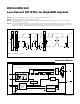
Figure 1. Data Transfer on I
2
C Serial Bus
Functional Diagram
SCL
NOTE: TIMING IS REFERENCED TO V
ILMAX
AND V
IHMIN
.
SDA
STOP START REPEATED
START
t
BUF
t
HD:STA
t
HD:DAT
t
SU:DAT
t
SU:STO
t
HD:STA
t
SP
t
SU:STA
t
HIGH
t
R
t
F
t
LOW
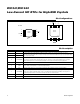
DS1341/DS1342
P
N
N
N
/4 /32 EXTSYNC
CONTROL LOGIC
OSC-1Hz
ALARM AND
CONTROL REGISTERS
CLOCK AND
CALENDAR REGISTERS
/2
128Hz OSC-1Hz
SQW/INTB
CLKIN/INTA
X1
X2
SCL
SDA
4.096kHz
8.192kHz
32.768kHz
MUX/
BUFFER
DIVIDER
EXT-1Hz
V
CC
SERIAL BUS
INTERFACE AND
ADDRESS
REGISTER