
Datasheet


I
2
C RTC with Trickle Charger
6 Maxim Integrated
DS1340
Detailed Description
The DS1340 is a low-power clock/calendar with a trickle
charger. Address and data are transferred serially
through a I
2
C bidirectional bus. The clock/calendar pro-
vides seconds, minutes, hours, day, date, month, and
year information. The date at the end of the month is
automatically adjusted for months with fewer than 31
days, including corrections for leap year. The DS1340
has a built-in power-sense circuit that detects power fail-
ures and automatically switches to the backup supply.
Power Control
The power-control function is provided by a precise,
temperature-compensated voltage reference and a
comparator circuit that monitors the V
CC
level. The
device is fully accessible and data can be written and
read when V
CC
is greater than V
PF
. However, when V
CC
falls below V
PF
, the internal clock registers are blocked
from any access. If V
PF
is less than V
BACKUP
, the
device power is switched from V
CC
to V
BACKUP
when
V
CC
drops below V
PF
. If V
PF
is greater than V
BACKUP
,
the device power is switched from V
CC
to V
BACKUP
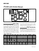
Pin Description
PIN
816
NAME FUNCTION
1 — X1
2 — X2
Connections for a Standard 32.768kHz Quartz Crystal. The internal oscillator circuitry is designed for
operation with a crystal having a specified load capacitance (C
L
) of 12.5pF. X1 is the input to the
oscillator and can optionally be connected to an external 32.768kHz oscillator. The output of the
internal oscillator, X2, is left unconnected if an external oscillator is connected to X1.
3 14 V
BACKUP
Connection for a Secondary Power Supply. For the 1.8V and 3V devices, V
BACKUP
must be held
between 1.3V and 3.7V for proper operation. Diodes placed in series between the supply and the input
pin may result in improper operation. V
BACKUP
can be as high as 5.5V on the 3.3V device.
This pin can be connected to a primary cell such as a lithium coin cell. Additionally, this pin can be
connected to a rechargeable cell or a super cap when used with the trickle-charge feature. UL
recognized to ensure against reverse charging when used with a lithium battery
(www.maximintegrated.com/qa/info/ul
).
4 15 GND Ground
5 16 SDA
Serial Data Input/Output. SDA is the data input/output for the I
2
C serial interface. The SDA pin is open
drain and requires an external pullup resistor.
6 1 SCL
Serial Clock Input. SCL is the clock input for the I
2
C interface and is used to synchronize data
movement on the serial interface.
7 2 FT/OUT
Frequency Test/Output. This pin is used to output either a 512Hz signal or the value of the OUT bit.
When the FT bit is logic 1, the FT/OUT pin toggles at a 512Hz rate. When the FT bit is logic 0, the
FT/OUT pin reflects the value of the OUT bit. This open-drain pin requires an external pullup resistor,
and operates with either V
CC
or V
BACKUP
applied. The pullup voltage can be up to 5.5V, regardless of
the voltage on V
CC
. If not used, this pin can be left unconnected.
8 3 V
CC
Primary Power Supply. When voltage is applied within normal limits, the device is fully accessible and
data can be written and read. When a backup supply is connected to the device and V
CC
is below V
PF
,
reads and writes are inhibited. However, the timekeeping function continues unaffected by the lower
input voltage.
— 4–13 N.C. No Connection. Must be connected to ground.
SUPPLY CONDITION
READ/WRITE
ACCESS
POWERED
BY
V
CC
< V
PF
,
V
CC
< V
BACKUP
No V
BAT
V
CC
< V
PF
,
V
CC
> V
BACKUP
No V
CC
V
CC
> V
PF
,
V
CC
< V
BACKUP
Yes V
CC
V
CC
> V
PF
,
V
CC
> V
BACKUP
Yes V
CC
Table 1. Power Control