
Datasheet


Address Map
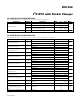
Table 3 shows the DS1340 address map. The RTC reg-
isters are located in address locations 00h to 06h, and
the control register is located at 07h. The trickle-charge
and flag registers are located in address locations 08h
to 09h. During a multibyte access of the timekeeping
registers, when the address pointer reaches 07h—the
end of the clock and control register space—it wraps
around to location 00h. Writing the address pointer to
the corresponding location accesses address locations
08h and 09h. After accessing location 09h, the address
pointer wraps around to location 00h. On a I
2
C START,
STOP, or address pointer incrementing to location 00h,
the current time is transferred to a second set of regis-
ters. The time information is read from these secondary
registers, while the clock may continue to run. This
eliminates the need to reread the registers in case the
main registers update during a read.
Clock and Calendar
The time and calendar information is obtained by read-
ing the appropriate register bytes. Table 3 shows the
RTC registers. The time and calendar data are set or
initialized by writing the appropriate register bytes. The
contents of the time and calendar registers are in the
binary-coded decimal (BCD) format. The day-of-week
I
2
C RTC with Trickle Charger
8 Maxim Integrated
DS1340
ADDRESS BIT 7 BIT 6 BIT 5 BIT 4 BIT 3 BIT 2 BIT 1 BIT 0 FUNCTION RANGE
00H EOSC 10 Seconds Seconds Seconds 00–59
01H X 10 Minutes Minutes Minutes 00–59
02H CEB CB 10 Hours Hours Century/Hours 0–1; 00–23
03H X X X X X Day Day 01–07
04H X X 10 Date Date Date 01–31
05H X X X 10 Month Month Month 01–12
06H 10 Year Year Year 00–99
07H OUT FT S CAL4 CAL3 CAL2 CAL1 CAL0 Control —
08H TCS3 TCS2 TCS1 TCS0 DS1 DS0 ROUT1 ROUT0 Trickle Charger —
09H OSF 0 0 0 0 0 0 0 Flag —
Table 3. Address Map
X = Read/Write bit
Note: Unless otherwise specified, the state of the registers is not defined when power is first applied.
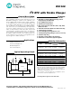
SERIAL
INTERFACE
AND ADDRESS
REGISTER
CONTROL
LOGIC
"C" VERSION ONLY
SCL
SDA
512Hz
MUX/
BUFFER
FT/OUT
USER BUFFER
(7 BYTES)
CLOCK AND
CALENDAR
REGISTERS
32,768Hz
1Hz
X1
POWER
CONTROL
V
CC
V
BACKUP
DIVIDER AND
CALIBRATION
CIRCUIT
X2
C
L
C
L
N
DS1340
Figure 5. Functional Diagram