
Datasheet
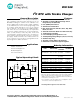


I
2
C RTC with Trickle Charger
Maxim Integrated 7
DS1340
when V
CC
drops below V
BACKUP
. The registers are
maintained from the V
BACKUP
source until V
CC
is
returned to nominal levels (Table 1). After V
CC
returns
above V
PF
, read and write access is allowed t
REC
.
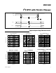
Oscillator Circuit
The DS1340 uses an external 32.768kHz crystal. The
oscillator circuit does not require any external resistors
or capacitors to operate. Table 2 specifies several crys-
tal parameters for the external crystal. Figure 3 shows a
functional schematic of the oscillator circuit. If using a
crystal with the specified characteristics, the startup
time is usually less than one second.
Clock Accuracy
The initial clock accuracy depends on the accuracy of
the crystal and the accuracy of the match between the
capacitive load of the oscillator circuit and the capaci-
tive load for which the crystal was trimmed. Additional
error is added by crystal frequency drift caused by
temperature shifts. External circuit noise coupled into
the oscillator circuit can result in the clock running fast.
Figure 4 shows a typical PC board layout for isolating
the crystal and oscillator from noise. Refer to
Application Note 58: Crystal Considerations with Dallas
Real-Time Clocks
(www.maximintegrated.com/RTCapps)
for detailed information.
DS1340C Only
The DS1340C integrates a standard 32,768Hz crystal
into the package. Typical accuracy with nominal V
CC
and +25°C is approximately +15ppm. Refer to
Application Note 58 for information about crystal accu-
racy vs. temperature.
Operation
The DS1340 operates as a slave device on the serial
bus. Access is obtained by implementing a START
condition and providing a device identification code fol-
lowed by data. Subsequent registers can be accessed
sequentially until a STOP condition is executed. The
device is fully accessible and data can be written and
read when V
CC
is greater than V
PF
. However, when
V
CC
falls below V
PF
, the internal clock registers are
blocked from any access. If V
PF
is less than V
BACKUP
,
the device power is switched from V
CC
to V
BACKUP
when V
CC
drops below V
PF
. If V
PF
is greater than
V
BACKUP
, the device power is switched from V
CC
to
V
BACKUP
when V
CC
drops below V
BACKUP
. The regis-
ters are maintained from the V
BACKUP
source until V
CC
is returned to nominal levels. The functional diagram
(Figure 5) shows the main elements of the serial RTC.
PARAMETER SYMBOL MIN TYP MAX UNITS
Nominal
Frequency
f
O
32.768 kHz
Series Resistance ESR 80 kΩ
Load Capacitance C
L
12.5 pF
Table 2. Crystal Specifications*
*
The crystal, traces, and crystal input pins should be isolated
from RF generating signals. Refer to
Application Note 58:
Crystal Considerations for Dallas Real-Time Clocks
for addi-
tional specifications.
COUNTDOWN
CHAIN
RTC
X1
X2
C
L
1
C
L
2
CRYSTAL
RTC
REGISTERS
Figure 3. Oscillator Circuit Showing Internal Bias Network
CRYSTAL
X1
X2
GND
LOCAL GROUND PLANE (LAYER 2)
Figure 4. Layout Example