
Datasheet


DS1339 I
2
C Serial Real-Time Clock
15 of 20
TRICKLE CHARGER REGISTER (10h)
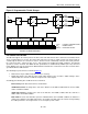
The simplified schematic in Figure 5 shows the basic components of the trickle charger. The trickle-charge select
(TCS) bits (bits 4 to 7) control the selection of the trickle charger. To prevent accidental enabling, only a pattern on
1010 enables the trickle charger. All other patterns disable the trickle charger. The trickle charger is disabled when
power is first applied. The diode-select (DS) bits (bits 2 and 3) select whether or not a diode is connected between
V
CC
and V
BACKUP
. The ROUT bits (bits 0 and 1) select the value of the resistor connected between V
CC
and V
BACKUP
.
Table 6 shows the bit values.
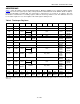
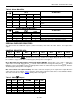
Table 6. Trickle Charger Register (10h)
BIT 7
BIT 6
BIT 5
BIT 4
BIT 3
BIT 2
BIT 1
BIT 0
FUNCTION
TCS3
TCS2
TCS1
TCS0
DS1
DS0
ROUT1
ROUT0
X
X
X
X
0
0
X
X
Disabled
X
X
X
X
1
1
X
X
Disabled
X
X
X
X
X
X
0
0
Disabled
1
0
1
0
0
1
0
1
No diode, 250
Ω
resistor
1
0
1
0
1
0
0
1
One diode, 250
Ω
resistor
1
0
1
0
0
1
1
0
No diode, 2k
Ω
resistor
1
0
1
0
1
0
1
0
One diode, 2k
Ω
resistor
1
0
1
0
0
1
1
1
No diode, 4k
Ω
resistor
1
0
1
0
1
0
1
1
One diode, 4k
Ω
resistor
0
0
0
0
0
0
0
0
Initial power-up values
Warning: The ROUT value of 250Ω must not be selected whenever V
CC
is greater than 3.63V.
The user determines diode and resistor selection according to the maximum current desired for battery or super
cap charging. The maximum charging current can be calculated as illustrated in the following example. Assume
that a 3.3V system power supply is applied to V
CC
and a super cap is connected to V
BACKUP
. Also assume that the
trickle charger has been enabled with a diode and resistor R2 between V
CC
and V
BACKUP
. The
maximum current I
MAX
would therefore be calculated as follows:
I
MAX
= (3.3V - diode drop) / R2 ≈ (3.3V - 0.7V) / 2kΩ ≈ 1.3mA
As the super cap or battery charges, the voltage drop between V
CC
and V
BACKUP
decreases and therefore the
charge current decreases.