
Datasheet


DS1339 I
2
C Serial Real-Time Clock
2 of 20
ABSOLUTE MAXIMUM RATINGS
Voltage Range on Any Pin Relative to Ground………………………………………………………………-0.3V to +6.0V
Operating Temperature Range (Noncondensing)………………………………………………………….-40°C to +85°C
Storage Temperature Range………………………………………………………………………………..-55°C to +125°C
Lead Temperature (soldering, 10s)...…………………………………………………………………………………+260°C
Soldering Temperature (reflow).……………………………………………………………………………………….+260°C
Stresses beyond those listed under “Absolute Maximum Ratings” may cause permanent damage to the device. These are stress ratings only,
and functional operation of the device at these or any other conditions beyond those indicated in the operational sections of the specifications is
not implied. Exposure to the absolute maximum rating conditions for extended periods may affect device reliability.
PACKAGE THERMAL CHARACTERISTICS (Note 1)
µSOP
Junction-to-Ambient Thermal Resistance (θ
JA
).…………………...……………………………………….206.3°C/W
Junction-to-Case Thermal Resistance (θ
JC
)……………………………………………………………………42°C/W
SO
Junction-to-Ambient Thermal Resistance (θ
JA
).……………………………………………………………….73°C/W
Junction-to-Case Thermal Resistance (θ
JC
)……………………………………………………………………23°C/W
Note 1: Package thermal resistances were obtained using the method described in JEDEC specification JESD51-7, using a four-layer
board. For detailed information on package thermal considerations, refer to
www.maxim-ic.com/thermal-tutorial.
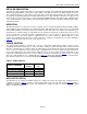
RECOMMENDED DC OPERATING CONDITIONS
(T
A
= -40°C to +85°C) (Note 2)
PARAMETER SYMBOL CONDITIONS MIN TYP MAX UNITS
Supply Voltage V
CC
DS1339-2 1.8 2.0 5.5
V
DS1339-3 2.7 3.0 5.5
DS1339-33 2.97 3.3 5.5
Backup Supply Voltage V
BACKUP
1.3 3.0 3.7 V
Logic 1 V
IH
0.7 x
V
CC
V
CC
+
0.3
V
Logic 0 V
IL
-0.3
+0.3 x
V
CC
V
Power-Fail Voltage V
PF
DS1339-2 1.58 1.70 1.80
V DS1339-3 2.45 2.59 2.70
DS1339-33 2.70 2.85 2.97