
Datasheet


DS1330Y/AB
8 of 10
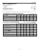
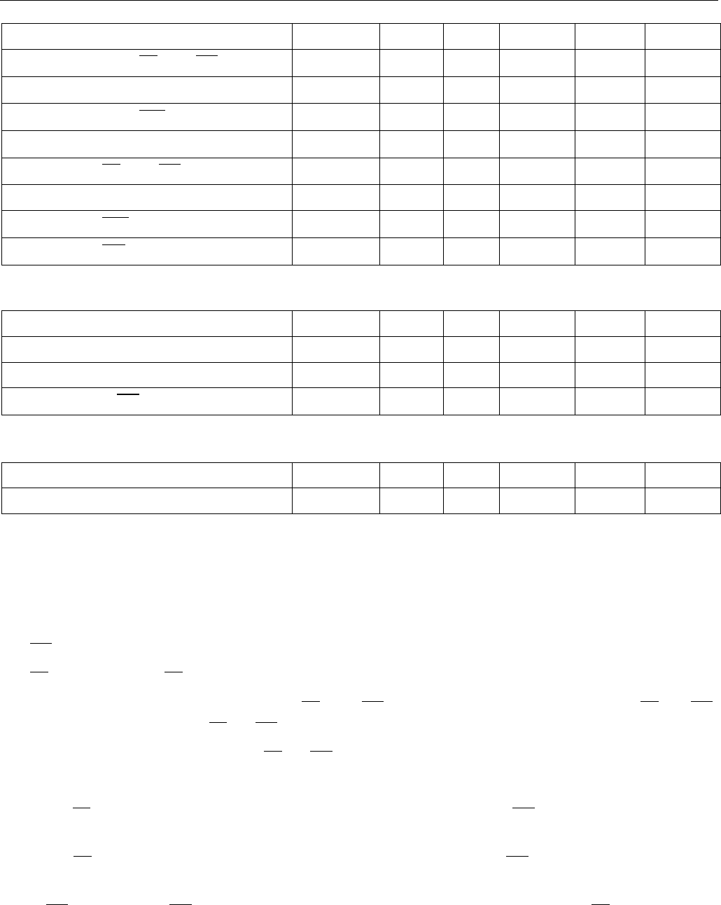
POWER-DOWN/POWER-UP TIMING (T
A
: See Note 10)
PARAMETER SYMBOL MIN TYP MAX UNITS NOTES
V
CC
Fail Detect to
CE
and
WE
Inactive
t
PD
1.5
µs
11
V
CC
slew from V
TP
to 0V t
F
150
µs
V
CC
Fail Detect to
RST
Active
t
RPD
15
µs
14
V
CC
slew from 0V to V
TP
t
R
150
µs
V
CC
Valid to
CE
and
WE
Inactive
t
PU
2 ms
V
CC
Valid to End of Write Protection t
REC
125 ms
V
CC
Valid to
RST
Inactive
t
RPU
150 200 350 ms 14
V
CC
Valid to
BW
Valid
t
BPU
1 s 14
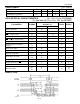
BATTERY WARNING TIMING (T
A
: See Note 10)
PARAMETER SYMBOL MIN TYP MAX UNITS NOTES
Battery Test Cycle t
BTC
24 hr
Battery Test Pulse Width t
BTPW
1 s
Battery Test to
BW
Active
t
BW
1 s
(T
A
= +25°C)
PARAMETER SYMBOL MIN TYP MAX UNITS NOTES
Expected Data Retention Time t
DR
10 years 9
WARNING:
Under no circumstance are negative undershoots, of any amplitude, allowed when device is in battery
backup mode.
NOTES:
1.
WE
is high for a Read Cycle.
2.
OE
= V
IH
or V
IL
. If
OE
= V
IH
during write cycle, the output buffers remain in a high-impedance state.
3. t
WP
is specified as the logical AND of
CE
and
WE
. t
WP
is measured from the latter of
CE
or
WE
going low to the earlier of
CE
or
WE
going high.
4. t
DS
is measured from the earlier of
CE
or
WE
going high.
5. These parameters are sampled with a 5pF load and are not 100% tested.
6. If the
CE
low transition occurs simultaneously with or latter than the
WE
low transition, the output
buffers remain in a high-impedance state during this period.
7. If the
CE
high transition occurs prior to or simultaneously with the
WE
high transition, the output
buffers remain in high-impedance state during this period.
8. If
WE
is low or the
WE
low transition occurs prior to or simultaneously with the
CE
low transition,
the output buffers remain in a high-impedance state during this period.