
Datasheet


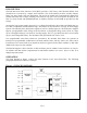
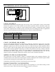
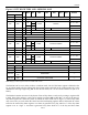
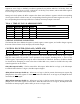
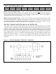
Table Of Contents
- BENEFITS AND FEATURES
- ORDERING INFORMATION
- DESCRIPTION
- Figure 1. BLOCK DIAGRAM
- CLOCK ACCURACY
- CLOCK, CALENDAR, AND ALARM
- WRITING TO THE CLOCK REGISTERS
- READING FROM THE CLOCK REGISTERS
- FUNCTION
- BIT7
- 1Hz (1Hz Output Enable) – This bit controls the 1Hz output. When this bit is a logic 1, the 1Hz output is enabled. When this bit is a logic 0, the 1Hz output is high-Z.
- AIE0 (Alarm Interrupt Enable 0) – When set to a logic 1, this bit permits the interrupt 0 request flag (IRQF0) bit in the status register to assert . When the AIE0 bit is set to logic 0, the IRQF0 bit does not initiate the signal.
- AIE1 (Alarm Interrupt Enable 1) – When set to a logic 1, this bit permits the interrupt 1 request flag (IRQF1) bit in the status register to assert INT1. When the AIE1 bit is set to logic 0, the IRQF1 bit does not initiate an interrupt signal, and the...
- STATUS REGISTER (READ 10H)
- TRICKLE CHARGE REGISTER (READ 11H, WRITE 91H)
- Table 3. TRICKLE CHARGER RESISTOR AND DIODE SELECT
- POWER CONTROL
- Figure 4. POWER-SUPPLY CONFIGURATIONS
- SERIAL INTERFACE
- SERIAL PERIPHERAL INTERFACE (SPI)
- Figure 5. SERIAL CLOCK AS A FUNCTION OF MICROCONTROLLER
- CLOCK POLARITY (CPOL)
- ADDRESS AND DATA BYTES
- Figure 6. SPI SINGLE-BYTE WRITE
- Figure 7. SPI SINGLE-BYTE READ
- Figure 8. SPI MULTIPLE-BYTE BURST TRANSFER
- BIT7
- READING AND WRITING IN BURST MODE
- Burst mode is similar to a single-byte read or write, except that CE is kept high and additional SCLK cycles are sent until the end of the burst. The clock registers and the user RAM may be read or written in burst mode. When accessing the clock regis...
- 3-WIRE INTERFACE
- Figure 9. 3-WIRE SINGLE BYTE TRANSFER
- ABSOLUTE MAXIMUM RATINGS
- RECOMMENDED DC OPERATING CONDITIONS (TA = Over the operating range, unless otherwise specified.)
- CAPACITANCE (TA = +25C)
- Figure 10. TIMING DIAGRAM: 3-WIRE READ DATA TRANSFER
- Figure 11. TIMING DIAGRAM: 3-WIRE WRITE DATA TRANSFER
- SPI AC ELECTRICAL CHARACTERISTICS (TA = Over the operating range, unless otherwise specified.)
- Figure 12. TIMING DIAGRAM: SPI READ DATA TRANSFER
- Figure 13. TIMING DIAGRAM: SPI WRITE DATA TRANSFER
- NOTES:
- REVISION HISTORY
- SYMBOL
- PARAMETER
- SYMBOL
- SYMBOL
- PARAMETER
- SYMBOL
- PARAMETER

DS1306
Table 3. TRICKLE CHARGER RESISTOR AND DIODE SELECT
TCS
Bit 7
TCS
Bit 6
TCS
Bit 5
TCS
Bit 4
DS
Bit 3
DS
Bit 2
RS
Bit 1
RS
Bit 0
FUNCTION
X X X X X X 0 0 Disabled
X X X X 0 0 X X Disabled
X X X X 1 1 X X Disabled
1 0 1 0 0 1 0 1 1 Diode, 2kΩ
1 0 1 0 0 1 1 0 1 Diode, 4kΩ
1 0 1 0 0 1 1 1 1 Diode, 8kΩ
1 0 1 0 1 0 0 1 2 Diodes, 2kΩ
1 0 1 0 1 0 1 0 2 Diodes, 4kΩ
1 0 1 0 1 0 1 1 2 Diodes, 8kΩ
0 1 0 1 1 1 0 0 Initial power-on state
If RS is 00, the trickle charger is disabled independently of TCS.
Diode and resistor selection is determined by the user according to the maximum current desired for
battery or super cap charging. The maximum charging current can be calculated as illustrated in the
following example. Assume that a system power supply of 5V is applied to V
CC1
and a super cap is
connected to V
CC2
. Also assume that the trickle charger has been enabled with one diode and resister R1
between V
CC1
and V
CC2
. The maximum current I
MAX
would, therefore, be calculated as follows:
I
MAX
= (5.0V - diode drop) / R1 ≈ (5.0V - 0.7V) / 2kΩ ≈ 2.2mA
As the super cap charges, the voltage drop between V
CC1
and V
CC2
decreases and, therefore, the charge
current decreases.
POWER CONTROL
Power is provided through the V
CC1
, V
CC2
, and V
BAT
pins. Three different power supply configurations
are illustrated in Figure 4. Configuration 1 shows the DS1306 being backed up by a non-rechargeable
energy source such as a lithium battery. In this configuration, the system power supply is connected to
V
CC1
and V
CC2
is grounded. When V
CC
falls below V
BAT
the device switches into a low-current battery
backup mode. Upon power-up, the device switches from V
BAT
to V
CC
when V
CC
is greater than
V
BAT
+ 0.2V. The device is write-protected whenever it is switched to V
BAT
.
Configuration 2 illustrates the DS1306 being backed up by a rechargeable energy source. In this case, the
V
BAT
pin is grounded, V
CC1
is connected to the primary power supply, and V
CC2
is connected to the
secondary supply (the rechargeable energy source). The DS1306 operates from the larger of V
CC1
or
V
CC2
. When V
CC1
is greater than V
CC2
+ 0.2V (typical), V
CC1
powers the DS1306. When V
CC1
is less than
V
CC2
, V
CC2
powers the DS1306. The DS1306 does not write-protect itself in this configuration.
Configuration 3 shows the DS1306 in battery-operate mode, where the device is powered only by a single
battery. In this case, the V
CC1
and V
BAT
pins are grounded and the battery is connected to the V
CC2
pin.
Only these three configurations are allowed. Unused supply pins must be grounded.
9 of 22