
Datasheet


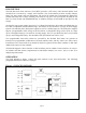
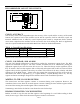
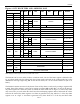
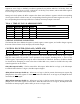
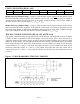
Table Of Contents
- BENEFITS AND FEATURES
- ORDERING INFORMATION
- DESCRIPTION
- Figure 1. BLOCK DIAGRAM
- CLOCK ACCURACY
- CLOCK, CALENDAR, AND ALARM
- WRITING TO THE CLOCK REGISTERS
- READING FROM THE CLOCK REGISTERS
- FUNCTION
- BIT7
- 1Hz (1Hz Output Enable) – This bit controls the 1Hz output. When this bit is a logic 1, the 1Hz output is enabled. When this bit is a logic 0, the 1Hz output is high-Z.
- AIE0 (Alarm Interrupt Enable 0) – When set to a logic 1, this bit permits the interrupt 0 request flag (IRQF0) bit in the status register to assert . When the AIE0 bit is set to logic 0, the IRQF0 bit does not initiate the signal.
- AIE1 (Alarm Interrupt Enable 1) – When set to a logic 1, this bit permits the interrupt 1 request flag (IRQF1) bit in the status register to assert INT1. When the AIE1 bit is set to logic 0, the IRQF1 bit does not initiate an interrupt signal, and the...
- STATUS REGISTER (READ 10H)
- TRICKLE CHARGE REGISTER (READ 11H, WRITE 91H)
- Table 3. TRICKLE CHARGER RESISTOR AND DIODE SELECT
- POWER CONTROL
- Figure 4. POWER-SUPPLY CONFIGURATIONS
- SERIAL INTERFACE
- SERIAL PERIPHERAL INTERFACE (SPI)
- Figure 5. SERIAL CLOCK AS A FUNCTION OF MICROCONTROLLER
- CLOCK POLARITY (CPOL)
- ADDRESS AND DATA BYTES
- Figure 6. SPI SINGLE-BYTE WRITE
- Figure 7. SPI SINGLE-BYTE READ
- Figure 8. SPI MULTIPLE-BYTE BURST TRANSFER
- BIT7
- READING AND WRITING IN BURST MODE
- Burst mode is similar to a single-byte read or write, except that CE is kept high and additional SCLK cycles are sent until the end of the burst. The clock registers and the user RAM may be read or written in burst mode. When accessing the clock regis...
- 3-WIRE INTERFACE
- Figure 9. 3-WIRE SINGLE BYTE TRANSFER
- ABSOLUTE MAXIMUM RATINGS
- RECOMMENDED DC OPERATING CONDITIONS (TA = Over the operating range, unless otherwise specified.)
- CAPACITANCE (TA = +25C)
- Figure 10. TIMING DIAGRAM: 3-WIRE READ DATA TRANSFER
- Figure 11. TIMING DIAGRAM: 3-WIRE WRITE DATA TRANSFER
- SPI AC ELECTRICAL CHARACTERISTICS (TA = Over the operating range, unless otherwise specified.)
- Figure 12. TIMING DIAGRAM: SPI READ DATA TRANSFER
- Figure 13. TIMING DIAGRAM: SPI WRITE DATA TRANSFER
- NOTES:
- REVISION HISTORY
- SYMBOL
- PARAMETER
- SYMBOL
- SYMBOL
- PARAMETER
- SYMBOL
- PARAMETER

DS1306
STATUS REGISTER (READ 10H)
BIT7
BIT6
BIT5
BIT4
BIT3
BIT2
BIT1
BIT0
0
0
0
0
0
0
IRQF1
IRQF0
IRQF0 (Interrupt 0 Request Flag) – A logic 1 in the interrupt request flag bit indicates that the current
time has matched the Alarm 0 registers. If the AIE0 bit is also a logic 1, the
INT0
pin goes low. IRQF0 is
cleared when the address pointer goes to any of the Alarm 0 registers during a read or write. IRQF0 is
activated when the device is powered by V
CC1
, V
CC2
, or V
BAT
.
IRQF1 (Interrupt 1 Request Flag) – A logic 1 in the interrupt request flag bit indicates that the current
time has matched the Alarm 1 registers. If the AIE1 bit is also a logic 1, the INT1 pin generates a 62.5ms
active-high pulse. IRQF1 is cleared when the address pointer goes to any of the alarm 1 registers during a
read or write. IRQF1 is activated only when the device is powered by V
CC2
or V
BAT
.
TRICKLE CHARGE REGISTER (READ 11H, WRITE 91H)
This register controls the trickle charge characteristics of the DS1306. The simplified schematic of Figure
3 shows the basic components of the trickle charger. The trickle charge select (TCS) bits (bits 4–7)
control the selection of the trickle charger. In order to prevent accidental enabling, only a pattern of 1010
enables the trickle charger. All other patterns disable the trickle charger. The DS1306 powers up with the
trickle charger disabled. The diode select (DS) bits (bits 2–3) select whether one diode or two diodes are
connected between V
CC1
and V
CC2
. The diode select (DS) bits (bits 2–3) select whether one diode or two
diodes are connected between V
CC1
and V
CC2
. The resistor select (RS) bits select the resistor that is
connected between V
CC1
and V
CC2
. The resistor and diodes are selected by the RS and DS bits as shown
in Table 3.
Figure 3. PROGRAMMABLE TRICKLE CHARGER
8 of 22