
Datasheet


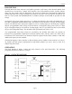
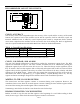
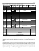
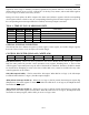
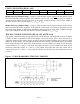
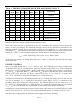
Table Of Contents
- BENEFITS AND FEATURES
- ORDERING INFORMATION
- DESCRIPTION
- Figure 1. BLOCK DIAGRAM
- CLOCK ACCURACY
- CLOCK, CALENDAR, AND ALARM
- WRITING TO THE CLOCK REGISTERS
- READING FROM THE CLOCK REGISTERS
- FUNCTION
- BIT7
- 1Hz (1Hz Output Enable) – This bit controls the 1Hz output. When this bit is a logic 1, the 1Hz output is enabled. When this bit is a logic 0, the 1Hz output is high-Z.
- AIE0 (Alarm Interrupt Enable 0) – When set to a logic 1, this bit permits the interrupt 0 request flag (IRQF0) bit in the status register to assert . When the AIE0 bit is set to logic 0, the IRQF0 bit does not initiate the signal.
- AIE1 (Alarm Interrupt Enable 1) – When set to a logic 1, this bit permits the interrupt 1 request flag (IRQF1) bit in the status register to assert INT1. When the AIE1 bit is set to logic 0, the IRQF1 bit does not initiate an interrupt signal, and the...
- STATUS REGISTER (READ 10H)
- TRICKLE CHARGE REGISTER (READ 11H, WRITE 91H)
- Table 3. TRICKLE CHARGER RESISTOR AND DIODE SELECT
- POWER CONTROL
- Figure 4. POWER-SUPPLY CONFIGURATIONS
- SERIAL INTERFACE
- SERIAL PERIPHERAL INTERFACE (SPI)
- Figure 5. SERIAL CLOCK AS A FUNCTION OF MICROCONTROLLER
- CLOCK POLARITY (CPOL)
- ADDRESS AND DATA BYTES
- Figure 6. SPI SINGLE-BYTE WRITE
- Figure 7. SPI SINGLE-BYTE READ
- Figure 8. SPI MULTIPLE-BYTE BURST TRANSFER
- BIT7
- READING AND WRITING IN BURST MODE
- Burst mode is similar to a single-byte read or write, except that CE is kept high and additional SCLK cycles are sent until the end of the burst. The clock registers and the user RAM may be read or written in burst mode. When accessing the clock regis...
- 3-WIRE INTERFACE
- Figure 9. 3-WIRE SINGLE BYTE TRANSFER
- ABSOLUTE MAXIMUM RATINGS
- RECOMMENDED DC OPERATING CONDITIONS (TA = Over the operating range, unless otherwise specified.)
- CAPACITANCE (TA = +25C)
- Figure 10. TIMING DIAGRAM: 3-WIRE READ DATA TRANSFER
- Figure 11. TIMING DIAGRAM: 3-WIRE WRITE DATA TRANSFER
- SPI AC ELECTRICAL CHARACTERISTICS (TA = Over the operating range, unless otherwise specified.)
- Figure 12. TIMING DIAGRAM: SPI READ DATA TRANSFER
- Figure 13. TIMING DIAGRAM: SPI WRITE DATA TRANSFER
- NOTES:
- REVISION HISTORY
- SYMBOL
- PARAMETER
- SYMBOL
- SYMBOL
- PARAMETER
- SYMBOL
- PARAMETER

DS1306
registers is set to a logic 1. Similarly, an alarm is generated every minute when bit 7 of the day, hour, and
minute alarm registers is set to a logic 1. When bit 7 of the day, hour, minute, and seconds alarm registers
is set to a logic 1, an alarm occurs every second.
During each clock update, the RTC compares the Alarm 0 and Alarm 1 registers with the corresponding
clock registers. When a match occurs, the corresponding alarm flag bit in the status register is set to a 1. If
the corresponding alarm interrupt enable bit is enabled, an interrupt output is activated.
Table 2. TIME-OF-DAY ALARM MASK BITS
ALARM REGISTER MASK BITS (BIT 7)
FUNCTION
SECONDS
MINUTES
HOURS
DAYS
1
1
1
1
Alarm once per second
0
1
1
1
Alarm when seconds match
0
0
1
1
Alarm when minutes and seconds match
0
0
0
1
Alarm hours, minutes, and seconds match
0
0
0
0
Alarm day, hours, minutes and seconds match
SPECIAL PURPOSE REGISTERS
The DS1306 has three additional registers (control register, status register, and trickle charger register)
that control the real-time clock, interrupts, and trickle charger.
CONTROL REGISTER (READ 0Fh, WRITE 8Fh)
BIT7
BIT6
BIT5
BIT4
BIT3
BIT2
BIT1
BIT0
0
WP
0
0
0
1Hz
AIE1
AIE0
WP (Write Protect) – Before any write operation to the clock or RAM, this bit must be logic 0. When
high, the write protect bit prevents a write operation to any register, including bits 0, 1, and 2 of the
control register. Upon initial power-up, the state of the WP bit is undefined. Therefore, the WP bit should
be cleared before attempting to write to the device. When WP is set, it must be cleared before any other
control register bit can be written.
1Hz (1Hz Output Enable) – This bit controls the 1Hz output. When this bit is a logic 1, the 1Hz output
is enabled. When this bit is a logic 0, the 1Hz output is high-Z.
AIE0 (Alarm Interrupt Enable 0) – When set to a logic 1, this bit permits the interrupt 0 request flag
(IRQF0) bit in the status register to assert
INT0
. When the AIE0 bit is set to logic 0, the IRQF0 bit does
not initiate the
INT0
signal.
AIE1 (Alarm Interrupt Enable 1) – When set to a logic 1, this bit permits the interrupt 1 request flag
(IRQF1) bit in the status register to assert INT1. When the AIE1 bit is set to logic 0, the IRQF1 bit does
not initiate an interrupt signal, and the INT1 pin is set to a logic 0 state.
7 of 22